differential amplifier

Thread Starter

anhnha

Joined Apr 19, 2012
904
Because if we neglecting channel length modulation, the impudence looking into the M9 source is indeed equal to 1/gm.
I ignored that effect in my calculation. However, the voltage at drain of Ṃ̣̣̣̣̣̣̣̀̀9 (Vg) is not at ground in ac model.
For example, in your picture, if the voltage at D is zero, then the input impedance is indeed 1/gm. But actually, it is not zero and Zin = RD + 1/gm.

Ah, I realize my mistake now. Zin ₫ Vx/Ix is still 1/gm. I did draw the model as in your picture. However, I also make a mistake in calculating Zin. I thought Zin is only equal to 1/gm if VD = 0V.
 

Jony130

Joined Feb 17, 2009
5,601
So as we established the capacitor current is equal to
Ifb = Vout/(1/gm + 1/sC). But this current at M9 drain is seen as a current source current. Because drain behavior just like a current source.
I thought Zin is only equal to 1/gm if VD = 0V.
No, VD can be larger then 0V.
Don't forget that the ideal DC voltage source has 0Ω internal resistance.
And that's why AC-signals are shorted by DC voltage source.
DC voltage is always constant so for any change in current there is non change in voltage. So there is 0 Ohm internal resistance.
And additional in real life circuit we always uses a bypass capacitor connect parallel to DC Voltage. And this capacitor will short all AC-signal to the ground. Because the large-value capacitor is a short for AC-signal.
 

Thread Starter

anhnha

Joined Apr 19, 2012
904
Jony, could you explain about DC level shift here?
Or could you post some links explaining about that?
I searched a lot but found nothing.
 

Jony130

Joined Feb 17, 2009
5,601
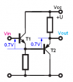
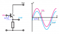
Here you have the simplest example of a DC level shifter circuit.

0.1.PNG

As you can see we use voltage follower circuit.
As you know the voltage at output (emitter) is shifted by 0.7V. So we can say that T1 is a DC level shifter. But we can add another transistor to compensate this shift.
0.2.PNG

I hope you see that T2 is a also a DC-level shifter. And thanks to this Vin = Vout. So T1 is a DC level shifter and T2 is a compensating DC level shifter. I hope that you understand this know.
 
Last edited:

Thread Starter

anhnha

Joined Apr 19, 2012
904
Thank you very much, Jony.
That explanation is really clear.
I will try to explain the DC level shift in the circuit above.
1. The voltage at the drain of Q2 will be lower than the voltage at the gate of Q2 an amount of Vth.
(DC level shift)
2. The voltage at drain of Q2C will be higher than the voltage at the source of Q2C an amount of Vth (Vds_min).
(compensating DC level shift)
I am confused about the function of Q2C and Q2.
I think they are not really put there to do these functions as their main tasks.
I think the main function of Q1 and Q2 is to amplify input signal not DC level shift.
I am not sure the function of Q1C and Q2C.
Are they used only for compensating DC level shift?
BTW, why do we need the high DC voltage at the output?
 

Thread Starter

anhnha

Joined Apr 19, 2012
904
I would like to ask another question.
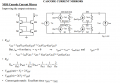
In that slide (page 18) or from the picture below, the author calculated output impedance of MOS Cascode Current Mirror.
In that picture, the author says that iin= 0. I think that is inferred from the condition that iI = constant.
But when the the current mirror is used as load for differential amplifier then it is obvious that iin ≠0, right?
If so, how can we calculate output impedance?


As in the picture, we can see that in small signal model the current flowing in current mirror is not zero at all.
iin ≠ 0. So, can we still apply the output impedance above?


Attachments

Jony130

Joined Feb 17, 2009
5,601
I am confused about the function of Q2C and Q2.
I think they are not really put there to do these functions as their main tasks.
I think the main function of Q1 and Q2 is to amplify input signal not DC level shift.
I am not sure the function of Q1C and Q2C.
Are they used only for compensating DC level shift?
Yes you are right that we don't use folded cascode circuit to compensating DC level shift. And I really don't know why author even mention this "strange" DC level shift thing. You should really forget about this terminology.
Cascode = no miller effect

I would like to ask another question.
In that slide (page 18) or from the picture below, the author calculated output impedance of MOS Cascode Current Mirror.
In that picture, the author says that iin= 0. I think that is inferred from the condition that iI = constant.
But when the the current mirror is used as load for differential amplifier then it is obvious that iin ≠0, right?
If so, how can we calculate output impedance?
Isn't we always assume Vin = 0V or Iin = 0A when we want to find Rout?
 

Thread Starter

anhnha

Joined Apr 19, 2012
904
As in from the picture, the input voltage of differential amplifier is always separated into two components.
1. Common mode voltage (Vin1 + Vin2)/2
2. Differential voltage (Vin1 - Vin2)/2

Does common mode voltage will establish operating conditions for the circuit?
Common mode voltage will determine gm but Vin1 and Vin2 always changes and this means that gm also changes continuously?
Can we call differential voltage small signal?
It doesn't sound right to me.
For example:
Vin1 = 2V, Vin2 = 0V
(Vin1 + Vin2)/2 = 1V
(Vin1 - Vin2)/2 = 1V
The differential voltage is not small at all.
 

Thread Starter

anhnha

Joined Apr 19, 2012
904
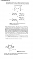
I just found the answer to my first question from Razavi book.
The operating point is set by current source not common mode voltage.
Here is an excerpt of it.


However, could you explain about the second question?
Is differential mode voltage small signal?
In the case of Vin1 = 2V, Vin2 =0V, the differential mode voltage is 1V that doesn't seem to be small at all.
 

Attachments

Jony130

Joined Feb 17, 2009
5,601
Is differential mode voltage small signal?
In the case of Vin1 = 2V, Vin2 =0V, the differential mode voltage is 1V that doesn't seem to be small at all.
Yes we treat the differential mode voltage as a small signal.
Why? Take the BJT first
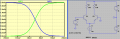
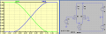
I plot Vd vs Ic for the differential amplifier and you will see that for Vd > ±120 mV. The input differential voltage is enough for almost all the current to be drawn by one of the transistors. This means that second transistor is cut-off.


So Vd for the linear region smaller than ±40 mV

For the MOS transistor we have a similar situation


For K = 1.3; Vt = 3.8V and Iss =1A we have Vd_max ≈ √(2*1A/(0.5 *1.3)) ≈ 1.7V.
or Vd_max = √2 * (Vgs - Vt) = 1.41*(4.68V - 3.8V) = 1.24V
And this is small compared to common mode voltage.
http://www-inst.eecs.berkeley.edu/~ee105/sp08/lectures/lecture24_2.pdf (page 5)
 

Attachments

Thread Starter

anhnha

Joined Apr 19, 2012
904
Thanks a lot, Jony.
Just one point that I don't understand.

or Vd_max = √2 * (Vgs - Vt) = 1.41*(4.68V - 3.8V) = 1.24V
According to above calculation, I think Vgs is 5.04V.
BTW, as in the lecture the equilibrium overdrive voltage is defined as
VGS‐VTH when M1 and M2 each carry a current of Iss/2.
From that I calculated Vgs - Vth = √(1A/(0.5 *1.3)) ≈ 1.24V.
So, Vgs = 1.24 + Vth = 1.24 + 3.8 = 5.04V.
Maybe I am missing something.
And now I have:
Differential mode voltage: Vd_max = 1.7V
Common mode voltage: Vg = Vgs + Vs_to_ground (the voltage across tail current source)
= 5.04 + Vs_to_ground >> 1.7V
Is that right?
Could you help me with the question?
Why do we need M4, M5 for this folded cascode? It seems to be used for biasing purpose. However, why don't we just use M3 to bias for all other transistors?


Jony130

Joined Feb 17, 2009
5,601
T
According to above calculation, I think Vgs is 5.04V.
BTW, as in the lecture the equilibrium overdrive voltage is defined as
VGS‐VTH when M1 and M2 each carry a current of Iss/2.
From that I calculated Vgs - Vth = √(1A/(0.5 *1.3)) ≈ 1.24V.
So, Vgs = 1.24 + Vth = 1.24 + 3.8 = 5.04V.
Maybe I am missing something.
Yes I made a small error in the firs equation.
But I'm sure that I have Vgs right

Vgs for Id1 = Id2 = 1A/2 = 0.5A is equal to

Vgs = Vt + √Id/(0.5*K) = 3.8V + √(0.5/0.65) = 4.677V

And don't forget that

Vd_max = Vg1 - Vgs2 = √2 * (Vgs - Vt)

From this

Vgs = Vt + Vd/√2 = 3.8V + 1.24/1.41 = 4.678V


And now I have:
Differential mode voltage: Vd_max = 1.7V
Common mode voltage: Vg = Vgs + Vs_to_ground (the voltage across tail current source)
= 5.04 + Vs_to_ground >> 1.7V
Is that right?
What? Isn't Vcm = (Vg1 + Vg2)/2 ?

Why do we need M4, M5 for this folded cascode? It seems to be used for biasing purpose.
Yes, M4 and M5 are use only for biasing.
However, why don't we just use M3 to bias for all other transistors?
Are you kidding me?
How can M3 current flow like this:
Vdd --->M2 ---> M7 source to drain ----> through M9 and M11 --->Vdd
 
Last edited:

Thread Starter

anhnha

Joined Apr 19, 2012
904
Thanks.
Yes I made a small error in the firs equation.
I believe you meant this.
For K = 1.3; Vt = 3.8V and Iss =1A we have Vd_max ≈ √(2*1A/1.3) ≈ 1.24V.
But I'm sure that I have Vgs right
Vgs for Id1 = Id2 = 1A/2 = 0.5A is equal to
Vgs = Vt + √Id/(0.5*K) = 3.8V + √(0.5/0.65) = 4.677V
Yes, I see now.
And don't forget that
Vd_max = Vg1 - Vgs = √2 * (Vgs - Vt)
Could you explain the red part?
From this
Vgs = Vt + Vd/√2 = 3.8V + 1.24/1.41 = 4.678V
This part is OK.
What? Isn't Vcm = (Vg1 - Vg2)/2 ?
Did you mean Vcm = (Vg1 + Vg2)/2?
How can you calculate Vcm here?
The maximum differential mode voltage is 1.24V with fixed biasing current and the specific transistor.
However, the common mode voltage will depend on input voltage and I don't know how to calculate it.
For example, with the transistor above, Vg1 = 2V, Vg2=0V, then Vcm = 1V.
Differential mode voltage is also 1V that is still in the linear range.
In this special case, the differential mode voltage is equal to common mode voltage but the differential mode voltage is still in the linear range.

If Vg1 = 4V, Vg2 = 0V.
Vcm = 2V, differential mode voltage = 2V and it is out of linear region.

Are you kidding me?
How can M3 current flow like this:
Vdd --->M2 ---> M7 source to drain ----> through M9 and M11 --->Vdd
Aha, I see it now. :D
The current direction is helpful.
 

Jony130

Joined Feb 17, 2009
5,601
And don't forget that
Vd_max = Vg1 - Vgs = √2 * (Vgs - Vt) Could you explain the red part?
Another silly mistake

Vd_max = Vg1 - Vg2 = √2 * (Vgs - Vt)

Did you mean Vcm = (Vg1 + Vg2)/2?
How can you calculate Vcm here?
The maximum differential mode voltage is 1.24V with fixed biasing current and the specific transistor.
However, the common mode voltage will depend on input voltage and I don't know how to calculate it.
For example, with the transistor above, Vg1 = 2V, Vg2=0V, then Vcm = 1V.
Differential mode voltage is also 1V that is still in the linear range.
In this special case, the differential mode voltage is equal to common mode voltage but the differential mode voltage is still in the linear range.

If Vg1 = 4V, Vg2 = 0V.
Vcm = 2V, differential mode voltage = 2V and it is out of linear region.
Yes, Vcm is the average of the two input voltages.
Vcm = (Vg1 + Vg2)/2

To find maximum input CM voltage you need to short g1 with g2 (Vd = 0V) and find Vcm needed for transistors to start leaving the saturation region.
 

Thread Starter

anhnha

Joined Apr 19, 2012
904
Jony, does this folded cascode amplifier still work if M6 and M7 are removed?
From output impedance formula, Rout is higher with M7. Is this the purpose of M7?
 

Jony130

Joined Feb 17, 2009
5,601
No this circuit will not work without M6 and M7. M6 and M7 are cascode transistor.
And cascode eliminates the miller effect and thus contributes to a much higher bandwidth.
 

Thread Starter

anhnha

Joined Apr 19, 2012
904
No this circuit will not work without M6 and M7. M6 and M7 are cascode transistor.
Things seem to be confusing now.
I don't see the functions of M6 and M7 except for increasing output impedance and reducing Miller effect.
 

Jony130

Joined Feb 17, 2009
5,601
What about input cm voltage range and this DC level shifting stuff?
Try to compare cm voltage for the ordinary cascode differential amp.
Also notice that thanks to this "DC level shifting" we have a one stage op amp. And we can apply negative feedback directly (we can short M2 gate and output to create voltage follower). Can we do this with the ordinary cascode differential amp? Of course not, we need to add additional stages to be able to do so.
 
Top