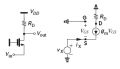
differential amplifier

Thread Starter

anhnha

Joined Apr 19, 2012
904
But do you understand why in "single" current mirror (without M3 and M4)
Vds1 = Vgs2?
And you don't need to hurry, because I need to go to sleep now.
It is clear from the picture! Because drain of M1 and gate of M2 are connected to each other.

And you don't need to hurry, because I need to go to sleep now.
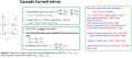
I will try to read phase margin and stability in the time and ask you later. :)
 

Jony130

Joined Feb 17, 2009
5,601
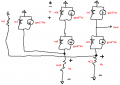
The problem now i how to prove Vds1 = Vds3 and Vds2 = Vds4
For me it's obvious that Vds1 = Vds3 and I don't need any prove. Why?
Because if we assume that all transistor are identical then M1 and M3 must have the same Vgs voltage. Vds1=Vgs1; Vds3=Vgs3.
Why they must have the same Vgs voltage? Because M1 and M3 are connected in series. And this means that Id1 = Id3 and this can only by true if Vgs1 = Vgs3.
If you don't believe me solve to I1 current in this circuit


Here is the small signal model for error amplifier.
The article says that ro1 is the output resistance of the error amplifier.
Please tell me how can I calculate ro1.
Hmm, You don't recognize this circuit. We already find ro1 for very similar circuit in post 9.
For my ro1 ≈ ro7||(gm9 * ro9)*ro2||ro11 ≈ ro7
Req - is load equivalent resistance = (R1+R2)||RL
Cg - Cdg9 but I'm not so sure about that.
I also don't fully understand this small signal model show in fig7.
 

Attachments

Last edited:

Thread Starter

anhnha

Joined Apr 19, 2012
904
Hi again, Jony.

For me it's obvious that Vds1 = Vds3 and I don't need any prove. Why?
Because if we assume that all transistor are identical then M1 and M3 must have the same Vgs voltage. Vds1=Vgs1; Vds3=Vgs3.
To me the circuit is not completely symmetrical. Q1 and Q3 are in different positions, one stacked with the other.
To be symmetrical they have to be arranged in a way that they have the same effect from other components.

Why they must have the same Vgs voltage? Because M1 and M3 are connected in series. And this means that Id1 = Id3 and this can only by true if Vgs1 = Vgs3.
The problem here is that you didn't take channel length modulation into account.
Ignore the channel length modulation effect, Vgs1 = Vgs3, as you said.

However, are they still equal if we consider the channel length modulation?

Hmm, You don't recognize this circuit. We already find ro1 for very similar circuit in post 9.
For my ro1 ≈ ro7||(gm9 * ro9)*ro2||ro11 ≈ ro7
Req - is load equivalent resistance = (R1+R2)||RL
Cg - Cdg9 but I'm not so sure about that.
I also don't fully understand this small signal model show in fig7.
Thanks. I also don't know why ifb is modeled as a current source between Vg and ground. ifb is the current flowing through Cc. Could you explain?
 

Jony130

Joined Feb 17, 2009
5,601
Hi again, Jony.
To me the circuit is not completely symmetrical. Q1 and Q3 are in different positions, one stacked with the other.
To be symmetrical they have to be arranged in a way that they have the same effect from other components.
The problem here is that you didn't take channel length modulation into account.
Ignore the channel length modulation effect, Vgs1 = Vgs3, as you said.

However, are they still equal if we consider the channel length modulation?
If we all transistor are identical then M1 and M3 must have the same Vgs voltage. Vds1=Vgs1; Vds3=Vgs3. End of the story.
If you don't believe me, do the math yourself. You can even include channel length modulation effect in your calculation. Because until all transistor are identical we will have Vgs1 = Vgs3.
Because M1 and M3 are connected in series. And this means that Id1 must be equal to Id3 (I Kirchhoff's law).
Id1 = 0.5*Kp1*(Vgs1 - Vt1)^2 *(1 + λVds1)
Id3 = 0.5*Kp3*(Vgs3 - Vt3)^2 *(1 + λVds3)
And if we have identical transistor, we have
Kp1 = Kp3; Vt1 = Vt3, λ1 = λ3; So if Id1 = Id2 , Vgs also must be equal.

Thanks. I also don't know why ifb is modeled as a current source between Vg and ground. ifb is the current flowing through Cc. Could you explain?
It seems that ifb is indeed the Cc capacitor current. This current is flowing from Vout through Cc directly into M9 source. And impedance of this node is 1/gm9 (CG amp). And this is why we have ifb current source connected to Vg.
 

Thread Starter

anhnha

Joined Apr 19, 2012
904
Thank you.

(Vgs1 - Vt)^2 *(1 + λVds1) = (Vgs3 - Vt)^2 *(1 + λVds3)

I know there is a solution is that Vgs1 = Vgs3 and Vds1 = Vds3. However, I can't prove that is the ONLY solution. :(
Maybe, I will need help to prove that later in a math forum.

It seems that ifb is indeed the Cc capacitor current. This current is flowing from Vout through Cc directly into M9 source. And impedance of this node is 1/gm9 (CG amp). And this is why we have ifb current source connected to Vg.
Well, it is much more complicated than I thought. :D

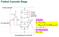
I just saw this circuit. Could you explain about the functions of these blocks?
1. DC level shift
2. Compensating DC level shift
3. Driven current generator


Attachments

Jony130

Joined Feb 17, 2009
5,601
Thank you.

(Vgs1 - Vt)^2 *(1 + λVds1) = (Vgs3 - Vt)^2 *(1 + λVds3)

I know there is a solution is that Vgs1 = Vgs3 and Vds1 = Vds3. However, I can't prove that is the ONLY solution. :(
Maybe, I will need help to prove that later in a math forum.
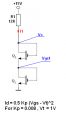
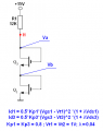
Here you have the solution for this circuit


And the solution


Of course only the solution marked in red can exist in our real world.
Do you know why?
Also check the LTspice simulation file.

I just saw this circuit. Could you explain about the functions of these blocks?
1. DC level shift
2. Compensating DC level shift
3. Driven current generator
I'm not going to help you with that. Because this leads you nowhere.
 

Attachments

Thread Starter

anhnha

Joined Apr 19, 2012
904
Thanks a lot.

Of course only the solution marked in red can exist in our real world.
Do you know why?
Because Vt = 1V and therefore, Vb should be greater than 1V.
Is that right?

How would you solve it if the 12K resistor now is replaced by an ideal current source, I0?

I'm not going to help you with that. Because this leads you nowhere.
Could you explain why? I thought it is similar to the one we discussed previously. :(
 

Jony130

Joined Feb 17, 2009
5,601
Because Vt = 1V and therefore, Vb should be greater than 1V.
Is that right?
Yes, right
How would you solve it if the 12K resistor now is replaced by an ideal current source, I0?
Simply replace (15 - Va)/R with I0.

Could you explain why? I thought it is similar to the one we discussed previously. :(
The topology is indeed similar, but the terminology use by the author to describe this circuit is rather strange.
And I don't have time to describe you all this stuff.
For example in ordinary cascode amp


The output voltage is taken from RL (no ground reference).
Also the output voltage swing is reduces because we have two transistors one on top of the other, which can reduce or limit the available output signal swing.

But if we use folded cascode we can DC shift the voltage.


So now our output voltage is at ground reference and also the output voltage swing has increase.
 

Thread Starter

anhnha

Joined Apr 19, 2012
904
That is interesting.

The output voltage is taken from RL (no ground reference).
Also the output voltage swing is reduces because we have two transistors one on top of the other, which can reduce or limit the available output signal swing.
Yes, I understood.
So now our output voltage is at ground reference and also the output voltage swing has increase.
Output voltage is at ground reference but it is upper limited? :confused:
 

Thread Starter

anhnha

Joined Apr 19, 2012
904
If we replace Rc1 with a current source the upper limited will be about 1V below Vcc.
For ordinary cascode amp the voltage swing is [VceQ1(sat) + VceQ2(sat) to Vdd]

For folded cascode the voltage swing is [0 to Vdd - VRc1 - VceQ2(sat)]
How can we know that VRc1 - VceQ2(sat) is smaller than VceQ1(sat) + VceQ2(sat)?
 

Jony130

Joined Feb 17, 2009
5,601
For ordinary cascode amp the voltage swing is [VceQ1(sat) + VceQ2(sat) to Vdd]

For folded cascode the voltage swing is [0 to Vdd - VRc1 - VceQ2(sat)]
How can we know that VRc1 - VceQ2(sat) is smaller than VceQ1(sat) + VceQ2(sat)?
I can't know that, because it's all depend on the particular circuit.
But in ordinary cascode Vbias will limit VceQ2(sat).
And Vbias must be larger than 3Vbe.
 

Thread Starter

anhnha

Joined Apr 19, 2012
904
It seems that ifb is indeed the Cc capacitor current. This current is flowing from Vout through Cc directly into M9 source. And impedance of this node is 1/gm9 (CG amp). And this is why we have ifb current source connected to Vg.
Sorry, I still don't get it.
1. Why Ifb doesn't go to M2 and end in ground?
2. It seems that Ifb flows through Cc to 1/gm and to ground. I don't know why we can model current source ifb from Vg to ground.
Could you explain more?
 

Jony130

Joined Feb 17, 2009
5,601
Sorry, I still don't get it.
1. Why Ifb doesn't go to M2 and end in ground?
Because M2 drain is a output not the input. Every transistor has to input.
At base/gate and at emitter/source. Collector/Drain are always output.
Also 1/gm9 is a much lower then ro2. So almost all current will flow through M9.

2. It seems that Ifb flows through Cc to 1/gm and to ground. I don't know why we can model current source ifb from Vg to ground.
Could you explain more?
I don't know the answer to this question. Also I think that author is cheating here. Why? Because the impudence looking into the M9 source is not equal to 1/gm9 if drain is not short to ground for AC signals.
 

Thread Starter

anhnha

Joined Apr 19, 2012
904
I don't know the answer to this question. Also I think that author is cheating here. Why? Because the impudence looking into the M9 source is not equal to 1/gm9 if drain is not short to ground for AC signals.
I have been always wondering why can they cheat at the paper like that. It is really disencouraging.
 

Jony130

Joined Feb 17, 2009
5,601
jony130 said:
Also I think that author is cheating here. Why? Because the impudence looking into the M9 source is not equal to 1/gm9 if drain is not short to ground for AC signals.
I have been always wondering why can they cheat at the paper like that. It is really disencouraging.
I made mistake in my last post. I must apologize the author. Because if we neglecting channel length modulation, the impudence looking into the M9 source is indeed equal to 1/gm.
 

Attachments

Top