Facebook
 Google
 GitHub
 Linkedin
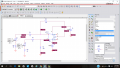
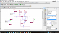
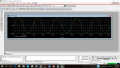
Hi, I am stuck on this problem where I need to plot the input and output waves. I also do not know how to simulate the 180 degree out of phase shift of v2. I have attatched both the questions and my PSPICE circuit.
Attachments
-
 558.7 KB Views: 12
 -
 159.4 KB Views: 13
 -
 115.9 KB Views: 13