Facebook
 Google
 GitHub
 Linkedin

I have designed and built a circuit that uses 2 CMOS analogue multiplexers - a DG408 and DG419 (both by Vishay). They are connected to an Atmega Microcontroller at 5V. The signals being switched are -5 to +5V audio freq signals.
The pin connections to the DG408:
A0/A1/A2: Atmega digital output pins
EN: 5V rail
-V: -12V rail
+V: +12V rail
inputs: -5 to +5V audio signal
output: to DG417 clean / filter circuit in
The pin connections to the DG419:
IN: Atmega digital output pin
-V: -12V rail
+V: +12V rail
VL: 5V rail
inputs: DG417 clean / filter circuit out (-5V to +5V)
output: to op amp gain/bias circuit
The DG419 works fine, but the DG408 always routes input 8 to the output, regardless of the state of the Atmega pins, which suggests that it is reading all of the A pins as held high. The voltage being read at the A pins (from the Atmega) are 0.02V for low and 4.9V for high, so well within CMOS ranges. The DG408 works fine if you manually connect the A pins to 5V rail and GND.
The key difference I can see between the 2 ICs is the VL rail on the DG419 which I guess gives it a reference level for logic high. The DG408 doesn't have this and I'm not sure how it derives a reference voltage, but the data sheet clearly states anything >2.4V for high and <0.8V for low.
If anyone with DG408 experience or interfacing TTL pins to CMOS devices, please let me know! I've done some googling and there are buffers that can go between the Atmega and DG408, but I can't see why they're necessary in this situation, as the voltages are within spec.
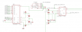
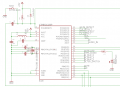
Schematic attached, annoyingly the Atmega is on a different sheet! Please note AGND and GND are tied together at present.
DG408 datasheet: https://www.vishay.com/docs/70062/dg408.pdf
DG417 datasheet: https://www.vishay.com/docs/70051/dg417.pdf
Happy to provide any other info if requested. thanks!
The pin connections to the DG408:
A0/A1/A2: Atmega digital output pins
EN: 5V rail
-V: -12V rail
+V: +12V rail
inputs: -5 to +5V audio signal
output: to DG417 clean / filter circuit in
The pin connections to the DG419:
IN: Atmega digital output pin
-V: -12V rail
+V: +12V rail
VL: 5V rail
inputs: DG417 clean / filter circuit out (-5V to +5V)
output: to op amp gain/bias circuit
The DG419 works fine, but the DG408 always routes input 8 to the output, regardless of the state of the Atmega pins, which suggests that it is reading all of the A pins as held high. The voltage being read at the A pins (from the Atmega) are 0.02V for low and 4.9V for high, so well within CMOS ranges. The DG408 works fine if you manually connect the A pins to 5V rail and GND.
The key difference I can see between the 2 ICs is the VL rail on the DG419 which I guess gives it a reference level for logic high. The DG408 doesn't have this and I'm not sure how it derives a reference voltage, but the data sheet clearly states anything >2.4V for high and <0.8V for low.
If anyone with DG408 experience or interfacing TTL pins to CMOS devices, please let me know! I've done some googling and there are buffers that can go between the Atmega and DG408, but I can't see why they're necessary in this situation, as the voltages are within spec.
Schematic attached, annoyingly the Atmega is on a different sheet! Please note AGND and GND are tied together at present.
DG408 datasheet: https://www.vishay.com/docs/70062/dg408.pdf
DG417 datasheet: https://www.vishay.com/docs/70051/dg417.pdf
Happy to provide any other info if requested. thanks!
Attachments
-
 15.6 KB Views: 9
 -
 19.9 KB Views: 6