Facebook
 Google
 GitHub
 Linkedin
Hello everyone, first of all thank you for taking the time to give this a peak!
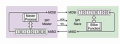
I am designing a PCB which is used as a HAT on a RaspberryPi and I am specifically designing it to use it for attaching a PMW3901 optical flow sensor.
I am unfamiliar with SPI sensors and have been googling around, which basically raised a question;
Am I supposed to add resistors on SPI tracks to reduce noise or is that overkill?
The distance between the connections and pathing on the PCB is less then 7 cm and would love to hear some advice on the topic.
After reading a lot of information online I am rather more confused then wise and have therefor turned to this forum.
Any assistance/insight is appreciated!