 Facebook
 Google
 GitHub
 Linkedin
Hello,
I'm designing a coplanar waveguide PCB, and I have a few questions about how to match the impedance along the PCB to be 50 Ohms.
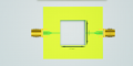
In the images I attached, there is a PCB model that I have designed so far, but without the dimensions of the trace and the ground plane spaces. Yellow color is exposed copper and the green color is the dielectric material. The SMA connector is attached horizontally to the PCB trace , the square hole in the middle is for attaching fabricated coplanar waveguide on a glass. I also attached a guide I read from, how the area near the SMA connector should look like for better match.
My issues are how to calculate the trace width, the ground spacing width, in the tapered area near the SMA, so the impedance will be 50 Ohms.
I understand that the center pin of the SMA is increasing the thickness of the copper, and because of that the area after the pin should become smaller.
To calculate coplanar cross sections with the same thickness is simple and there are a lot of calculators online, but when the SMA is added, I'm not sure what to do.
I'm new to this field of designing RF circuits, so if I wasn't clear or I didn't mention important information, please let me know.
Thank you for any help.
I'm designing a coplanar waveguide PCB, and I have a few questions about how to match the impedance along the PCB to be 50 Ohms.
In the images I attached, there is a PCB model that I have designed so far, but without the dimensions of the trace and the ground plane spaces. Yellow color is exposed copper and the green color is the dielectric material. The SMA connector is attached horizontally to the PCB trace , the square hole in the middle is for attaching fabricated coplanar waveguide on a glass. I also attached a guide I read from, how the area near the SMA connector should look like for better match.
My issues are how to calculate the trace width, the ground spacing width, in the tapered area near the SMA, so the impedance will be 50 Ohms.
I understand that the center pin of the SMA is increasing the thickness of the copper, and because of that the area after the pin should become smaller.
To calculate coplanar cross sections with the same thickness is simple and there are a lot of calculators online, but when the SMA is added, I'm not sure what to do.
I'm new to this field of designing RF circuits, so if I wasn't clear or I didn't mention important information, please let me know.
Thank you for any help.
Attachments
-
 371 KB Views: 9
 -
 216.8 KB Views: 9
 -
1.7 MB Views: 5


