Designing a Voltage Regulator

SgtWookie

Joined Jul 17, 2007
22,230
OK, after a bit of fiddling around, I've determined that some changes are necessary.

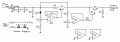
Neither Q1 nor Q2 has enough gain. I've replaced Q1 with a 2N4403. Q2 had to be replaced with a 2N6426 Darlington.

5.1v is not enough for D2; 5.6 would be minimal for a 2N2222, it had to be increased to 6.2v to match the base-emitter drop of the 2N6426. The 2n2222 simply didn't have enough gain.

Even with the changes I've made, current limiting from Q1 will only be effective down to about 0.1mA due to current flow via R6 through Q2, if R5 is still set to output 5v. Current limiting with the 2n2222 was far worse.

See the attached. If a Darlington with higher gain is used, R6 can be increased accordingly.
 

Attachments

Last edited:

Wendy

Joined Mar 24, 2008
23,421
You moved the op amp sense, it compensated for the BE drop. The 5.1V zener is available from Radio Shack.

I had the same thoughts about Q2. I figured lowest value for the resistor I felt we could get by with, but a Darlington solves all that. You can also use the TIP105 (overkill for the job) or qty 2 2N2222 wired as a Darlington.

The diodes CR3 and CR4 allow the op amp to stay away from the power supply rails, a bad thing.

R7 allows the Q2 to be correctly biased, even without a load. A good thing.

Thanks Wookie.

So it should look more like this...


Parts List:

U1 : 7809
U2 : LM324
Q1 : 2N4403
Q2 : 2N6427
C1 : 100µF
C2 : 0.1µF
CR1,3,4 : 1N4001
CR2 : 5.1V Zener
R1 : 91Ω ¼W
R2 : 2KΩ Variable
R3 : 6.2KΩ ¼W
R4 : 390Ω ¼W
R5 : 10KΩ Variable
R6 : 100KΩ ¼W
R7 : 10KΩ ¼W
 
Last edited:

SgtWookie

Joined Jul 17, 2007
22,230
OK, with that feedback, the output is sent into high frequency oscillations from 1v to 7v. Not good.

Need a way to provide feedback without causing excessive current flow. Might have to go to a FET.

The LM324 does not have rail-to-rail outputs; therefore there will always be SOME current flowing via R6 through the base-emitter junction. The transistor's base would have to be pulled down to 0v to stop the current flow. Not possible with the current components.
 

darin

Joined Nov 20, 2008
58
I have testing the circuit by using components which i am able to find. The circuit is able to produce a voltage of maximum 4.51V output voltage at a maximum current of 23.48mA at the output.

The components which i have made use which are different are:

Replacing LM324 with TL081CV
2 NPN C550CV to build the Darlington Pair
C558 PNP

Any suggestion to the connections?
 

msdmsd

Joined Nov 21, 2008
8
I'm going to abandon the thread I started about the power supply I needed since this is almost exactly what I'm looking for and the same people are working on it.

Is it possible to modify this to limit current between 20mA and 60mA?
 

Wendy

Joined Mar 24, 2008
23,421
I have testing the circuit by using components which i am able to find. The circuit is able to produce a voltage of maximum 4.51V output voltage at a maximum current of 23.48mA at the output.

The components which i have made use which are different are:

Replacing LM324 with TL081CV
2 NPN C550CV to build the Darlington Pair
C558 PNP

Any suggestion to the connections?
Which wiring diagram did you use? It sounds like Wookies, since 4.5V is way too low. It should reach the zener voltage, 5.1. You can measure this to verify.

For the range of current/voltage banana plugs and jacks should be fine.

The point of CR3 and CR4 is you will not go to rail to rail, so a cheap op amp should work. Is 1.2V from the negitave power supply not enough Wook? You'll note I put the op amp on the negitive power supply.

What kind of frequency are we talking about on the oscillation? Does adding an output cap or reducing the base resistor help? I truely don't understand why it would oscillate, the negitive feedback is pretty firm.
 

darin

Joined Nov 20, 2008
58
Which wiring diagram did you use? It sounds like Wookies, since 4.5V is way too low. It should reach the zener voltage, 5.1. You can measure this to verify.

For the range of current/voltage banana plugs and jacks should be fine.

The point of CR3 and CR4 is you will not go to rail to rail, so a cheap op amp should work. Is 1.2V from the negitave power supply not enough Wook? You'll note I put the op amp on the negitive power supply.

What kind of frequency are we talking about on the oscillation? Does adding an output cap or reducing the base resistor help? I truely don't understand why it would oscillate, the negitive feedback is pretty firm.

Hi, i made use of your first schematic but have the NPN transistor changed to a Darlington pair. I have measured the zener diode output and it measured 5.1V which is correct.

My aplogises as i did not connect up CR3 and CR4, when the 2 diodes are connected to the op amp, a voltage of 9V will be measured on the output along with a maximum of 23mA.

Just wonder, if i change the regulator at the input from 7809 to a 7805. Will i get a 5V output?
 
Last edited:

SgtWookie

Joined Jul 17, 2007
22,230
Just wonder, if i change the regulator at the input from 7809 to a 7805. Will i get a 5V output?
No, due to the voltage drop across the PN junctions in the transistors. Your maximum output voltage would then be around 3.74.

You can increase the output voltage from a 7805 regulator by adding resistance between the ground pin and GND. The ground pin has a nominal 5mA current, so every 100 Ohms of resistance added increases the output voltage by approximately 0.5v.

Note that the 78xx series regulators require a minimum of 10mA total current in order to provide guaranteed regulation of the output voltage. Approximately 5mA of that 10mA load is accounted for via the current of the GND terminal. You can ensure that the remaining 5mA current is drawn by using a resistor on the output terminal to ground; at most 200 Ohms per volt.
 

darin

Joined Nov 20, 2008
58
I don't know why you're substituting completely different components from what was specified.

Try the attached. You can get any/all of the parts from your local Radio Shack.
Yup i have to make use of whatever i can find first in school before i can make any orders as i am a student still However from ur simulation, i can see that it is performing to what is required.
 

darin

Joined Nov 20, 2008
58
I don't know why you're substituting completely different components from what was specified.

Try the attached. You can get any/all of the parts from your local Radio Shack.
I will like to know from the circuitry, what is the maximum current value can u reach at the output?
 

darin

Joined Nov 20, 2008
58
I don't know why you're substituting completely different components from what was specified.

Try the attached. You can get any/all of the parts from your local Radio Shack.
Hi wookie,

can u explain some how the circuitry works with the varies components selected for the design u did.

thanks
 

Wendy

Joined Mar 24, 2008
23,421
The OP wrote me to talk about some problems he's having, so I'll start off the conversation.

You should see a variable voltage on the base of Q1/wiper of R2. Try disconnecting the wiper from the pot (this is likely the problem, my fault).


Parts List:

U1 : 7809
U2 : LM324
Q1 : 2N2222
Q2 : 2N2907
C1 : 100µF
C2 : 0.1µF
CR1,3,4 : 1N4001
CR2 : 5.1V Zener
R1 : 91Ω ¼W
R2,5 : 2KΩ Variable
R3 : 6.2KΩ ¼W
R4 : 390Ω ¼W
R6,7 : 10KΩ ¼W
 

Attachments

Wendy

Joined Mar 24, 2008
23,421
I'm going to sketch another design, something a little simplier which should work. The problem is with less gain there is less flexiability on the resistors.


Parts List:

U1 : 7809
Q1 : 2N2907
Q2,3 : 2N6427 Qty 1
CR1 : 1N4001
R1 : 100Ω
R2 : 500Ω Variable
R3 : 1.0KΩ
R4 : 210Ω
R5 : 500Ω Variable
R6,7 : 10KΩ

You said something about using 10KΩ programmable pots. I'll put something up that's compatible with those next.
 

Attachments

Last edited:

Wendy

Joined Mar 24, 2008
23,421


Parts List:

U1 : 7809
U2 : LM324
Q1 : 2N2907
Q2,3 : 2N6427 Qty 1
CR1,3,4 : 1N4001
C1 : 100µF
C2 :0.1µF
R1 : 100Ω
R2,5 : 10KΩ Variable
R3 : 21KΩ
R4 : 4.3KΩ
R6 : 100KΩ
R7 : 10KΩ
R8 : 1KΩ

Theory of Operation

Q1 sets up a constant voltage across R1, which sets up a constant current on the Collector of Q1. If the current pulled from the load is less than the current programed into the constant current source then the transistor Q1 is turned fully on.

Q2/3 is an emitter follower, which is a basic voltage regulator. Since the resistors R4 and R5 are feed directly from a regulated voltage, the voltage on the wiper of R5 is also regulated without a load. The op amp barely loads R5, and has a low impedance output, which feeds Q2/3. We want the highest resistance possible between the op amp and the Base of Q2, since if the current regulator has dropped the collector of Q2/3 to a low voltage the Base Emitter of Q2/3 will feed the load. This is kept to a minimum with a large resistance.

CR2 and CR3 raise the voltage of ground from the op amps negitive power supply. This is to allow basic op amps, which can not handle the power supply directly on the inputs, to work the full range of adjustment.

The other 2 op amps should be connected as shown to prevent unwanted side effects, such as oscillation.
 

Attachments

Last edited:
Top