Designing a unviversal data logger using analog switches and PSOC5LP

Thread Starter

pratik bhagat

Joined Sep 12, 2018
17
Dear Guru's,
i am willing to design a data-logger for my project which will connect and log various sensor outputs. I need to connect themrocouple k type, rtd pt100 , 4-20ma current sensor and a 1-10volt output sensor. All these sensors swapable on any channel. And my datalogger will have 12 channels.

I decided to go with psoc 5lp and i am working on it. Internal psoc 5Lp can read and is suffiecient for 4 channels. And my datalogger has 16 channels. Also i want to log data in sd card and usb drive also a modbus RS232 slave / tcp ip slave connection is required. I have completed all the modules . But now i got stuck when it came to pin limitations of psoc5Lp. I already invested in this chip and other sensors. Also time has been invested.

So decided to finish the project by using one last component which will take care of the pin limitation. So i need a helping hand regarding the analog switch / mux which can be cost .

I am lot confused about the analog mux Rds at on and matching as i think it will be difficult if the mv drops due to rds.


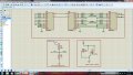
I need help to decide which analog switch /mux to be used . I am attaching the basic cirucitary for analog input section.


this is basic design for just four channel. I want to extend this to 16 channel. Is this circuit correct.
 

Attachments

ericgibbs

Joined Jan 29, 2010
18,849
hi pratik,
If I am reading the circuit diagram correctly are you considering trying pass a 20mA/40mA current thru the 4052 analog switch.?
Have you checked the power/current limits in the d/s?
E
AA1 15-Sep-18 09.54.gif
 
Last edited:

danadak

Joined Mar 10, 2018
4,057
I didnt understand i need to use differential inputs of thermocouple and rtd . Also 4-20ma and 0-10volt sensor ouput to be fed to psoc adc via mux. I need atmost 2 X 12 channels=24 pin of psco dedicately. Also need pins for sd card spi interface, then rs232 modbus aswell.
Typical I/O on a PSOC 5LP is 70+ pins.

I routed this, as you can see it routed and resources in right hand window
show 28 out of 72 pins used, leaving 44 pins for other stuff.

See attached.

Regards, Dana.
 

Attachments

Thread Starter

pratik bhagat

Joined Sep 12, 2018
17
hi pratik,
If I am reading the circuit diagram correctly are you considering trying pass a 20mA/40mA current thru the 4052 analog switch.?
Have you checked the power/current limits in the d/s?
E
View attachment 159932
Sir,
Yeah you right this will fry the switch. I was just simulating. As less component are in proteus. l will change the switches I just want to know whether this circuit will work
As signal conditioning is applied at stage two.

For 4/20 ma loop PSOC cannot generate the current loop, so you do
that externally and use external receiver to feed I/O from PSOC to loop.
So mux resistance is irrelevant

https://www.planetanalog.com/author.asp?section_id=3066&doc_id=563262.

Regards, Dana.
Learnt something new. Thanks Dana.
Dana my psoc will have four buttons spst , 12-16 channels interchangeble for any sensor input, sensors type rtd thermocouple 4-20ma and 0-5v 0-10v output sensor.
Please check I have attached my ciruitary. Yes some circutary is extracted from psoc examples
 
Last edited by a moderator:

Thread Starter

pratik bhagat

Joined Sep 12, 2018
17
Attachment here

MOD: No image.???
What type of file 'ext' are you trying to post.?


Dana,
Please scroll up to first post you will find the attachment.
 
Last edited by a moderator:

Thread Starter

pratik bhagat

Joined Sep 12, 2018
17
Do you still need the external muxes after what I showed you in post #3 ?

Regards, Dana.
Dear Dana,
I will share a complete design and block diagram . Please wait for today as it is sunday.(India)

Jpeg

Typical I/O on a PSOC 5LP is 70+ pins.

I routed this, as you can see it routed and resources in right hand window
show 28 out of 72 pins used, leaving 44 pins for other stuff.

See attached.

Regards, Dana.
Which psoc is this. I am using psoc5Lp 68 pin
 
Last edited by a moderator:

danadak

Joined Mar 10, 2018
4,057
I used the CY8C5868AXI-LP035, the standard project part used
when starting a PSOC design. 100 TQFP

I did a route on 68 QFN, and it used 28/48 I/O, eg. left another 20 for use.

Regards, Dana.
 

Thread Starter

pratik bhagat

Joined Sep 12, 2018
17
I used the CY8C5868AXI-LP035, the standard project part used
when starting a PSOC design. 100 TQFP

I did a route on 68 QFN, and it used 28/48 I/O, eg. left another 20 for use.

Regards, Dana.
Dear Dana,
Please can you please share psoc5LP 68qfn schematic.

Also I will share the Deposit.

Also I will share the block diagram and circuit diagram tommorow
 
Last edited by a moderator:

Thread Starter

pratik bhagat

Joined Sep 12, 2018
17
Dear Dana,
need updates on how to use all pins. Also can we use swd pins . And can you help , I need psoc 5lp Board layout need to know the bypass capacitors.
with this schematic i think i dont need external analog mux. But only problem with 0-10volt output sensor. I think i need to externally use voltage divider for 0-10volt and a shunt resistor for 4-20ma sensor.


Dana I was to also know whether removing the by pass capacitor will make no harm
 

danadak

Joined Mar 10, 2018
4,057
I think i need to externally use voltage divider for 0-10volt and a shunt resistor for 4-20ma sensor.
Yes to divider. Shunt R for 4/20 ma, yes, but that must result in a signal that meets
CM input range of A/D. Or you G and level shift it externally if its compliance range
is outside PSOC analog rails. If signal is inside CM rails you can use onchip OpAmp
and external R's to do the level shift.


SWD as GPIO -

Sets the Port 1 preferred program/debug interface (JTAG or SWD or SWD+SWV) that the chip enables by default for use after power up or reset. Setting to GPIO frees the pins for use as GPIOs but does not completely disable the debug interface for flash protection purposes. "Enable Device Protection" must be set for this purpose. For more information about programming and debugging options see the device data sheet or Technical Reference Manual (TRM).
In "Design wide resources" explorer window, "System" entry, there is a debug setting to
allow swd to be used as GPIO.

http://www.cypress.com/documentation/application-notes/an72382-using-psoc-3-and-psoc-5lp-gpio-pins


Board layout considerations (page 10) -

http://www.cypress.com/documentatio...nd-psoc-5lp-mixed-signal-circuit-board-layout

Dana I was to also know whether removing the by pass capacitor will make no harm
I recommend following the above recommendations.


Regards, Dana.
 
Last edited:

danadak

Joined Mar 10, 2018
4,057
Here is one approach to receiver. You could use PSOC onchip OpAmp(s)
to handle this. Note the schematic has an error, the + and - inputs are
swapped. Not the pin numbers, but what they connect to on this schematic.
+ should connect to 100K to ground and 100K to Out 4-20 ma. - should
connect to junction of 2 series 100K's


https://www.sensorsmag.com/components/implementing-a-4-ma-to-20-ma-sensor-interface

Regards, Dana.
 
Last edited:

danadak

Joined Mar 10, 2018
4,057
Here is a single supply version -

upload_2018-9-18_12-24-12.png

Note supply could be 5V, and use internal PSOC OpAmp.

Zener should be 3.0 V or 5.1 V to meet PSOC CM input limitations.

Regards, Dana.
 

Thread Starter

pratik bhagat

Joined Sep 12, 2018
17
Here is a single supply version -

View attachment 160121

Note supply could be 5V, and use internal PSOC OpAmp.

Zener should be 3.0 V or 5.1 V to meet PSOC CM input limitations.

Regards, Dana.
Dear Dana,
I am so glad that you are helping me with interest. Dana Why can't I just use shunt and zener+current limiter resistor .
Many of Arduino user have used this easy technique. Psoc can take input till 5.5 and delsigma has +- 6volt adc . A 200 ohm resistor keeps voltage below 4.5v. and a zener will do it's job
 

Thread Starter

pratik bhagat

Joined Sep 12, 2018
17
Wed pin onc
Yes to divider. Shunt R for 4/20 ma, yes, but that must result in a signal that meets
CM input range of A/D. Or you G and level shift it externally if its compliance range
is outside PSOC analog rails. If signal is inside CM rails you can use onchip OpAmp
and external R's to do the level shift.


SWD as GPIO -


In "Design wide resources" explorer window, "System" entry, there is a debug setting to
allow swd to be used as GPIO.

http://www.cypress.com/documentation/application-notes/an72382-using-psoc-3-and-psoc-5lp-gpio-pins


Board layout considerations (page 10) -

http://www.cypress.com/documentatio...nd-psoc-5lp-mixed-signal-circuit-board-layout


I recommend following the above recommendations.


Regards, Dana.
Swd once set a gpios. Can we further program the psoc using jtag?
 
Top