Facebook
 Google
 GitHub
 Linkedin
Hi everyone,
As I am working on this project solo, I have been using AI tools to assist with my custom power supply design, covering both the schematic design and PCB layout. Although the design has undergone multiple rounds of optimization and initial AI checks without flagging major issues, I am still quite concerned about potential blind spots. Given my limited design experience, I worry there may be critical oversights or design flaws that I've missed.
If you have some spare time, I would be incredibly grateful if you could review my design and share your professional feedback. Any advice on the schematic parameters, thermal management, EMC, or routing layout would be invaluable to me.
Thank you so very much for your time and help!
Key Specifications:
Input Voltage:Max stable input of 720V DC (Components selected with 1000V - 1200V margin).
Intermediate Bus Voltage:380V DC @ 0.58A.
Output: Two fully independent 12V DC channels, identical power rating per channel, with four output connectors. Total output power is **220W** (forced air cooled).
Switching Frequency: Both stages are synchronized/designed at 100 kHz.
Topology & Stage Architecture:
1. Pre-stage Inverted (Low-side) Buck Converter:
Topology: Non-isolated inverted Buck converter (low-side switch configuration) to step down the 720V DC input to a stable 380V DC intermediate bus.
Controller: U9 UCC28C43 current-mode PWM controller.
2. Downstream Isolated Stage (Active Clamp Flyback - ACF):
Topology: High-frequency Active Clamp Flyback (ACF) directly powered by the 380V intermediate bus.
Controller:U6 Joulwatt JW1551 HF active clamp controller.
Power Stage: U4 Integrated 650V GaN half-bridge IC JW1568K.
3. Secondary-Side Synchronous Rectification (SR):
Controller: Two independent MP6908AGJ(U3-U24) high-frequency SR controllers (one for each 12V channel).
Power Switches: Two HYG090N06LS1C2 MOSFETs (60V, ultra-low Rds(on))(Q1-Q4) in parallel per channel.
4. Feedback Loop & Isolation:
Mechanism:TL431 precision shunt regulator paired with a PC817 optocoupler.
Feedback Source: Sensed from the primary 12V/55W closed-loop channel on the secondary side, feeding back into the COMP pin of the primary-side JW1551 controller.
Y-Capacitor: Primary-to-secondary isolation Y-capacitor added.
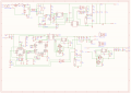
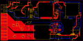
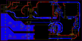
U16 is a PQ3220 inductor, which has an auxiliary winding to power the nearby optocoupler. U8 is a PQ3535 transformer. NET12 is the negative pole of the intermediate 380V DC bus.
U15 and U19 are NTC thermistors, FH3 is a fuse holder, R32 is a varistor, U14 is a safety capacitor, D2 is a gas discharge tube (GDT), L2 is a common-mode inductor, and C29 and C32 are Y-capacitors.
As I am working on this project solo, I have been using AI tools to assist with my custom power supply design, covering both the schematic design and PCB layout. Although the design has undergone multiple rounds of optimization and initial AI checks without flagging major issues, I am still quite concerned about potential blind spots. Given my limited design experience, I worry there may be critical oversights or design flaws that I've missed.
If you have some spare time, I would be incredibly grateful if you could review my design and share your professional feedback. Any advice on the schematic parameters, thermal management, EMC, or routing layout would be invaluable to me.
Thank you so very much for your time and help!
Key Specifications:
Input Voltage:Max stable input of 720V DC (Components selected with 1000V - 1200V margin).
Intermediate Bus Voltage:380V DC @ 0.58A.
Output: Two fully independent 12V DC channels, identical power rating per channel, with four output connectors. Total output power is **220W** (forced air cooled).
Switching Frequency: Both stages are synchronized/designed at 100 kHz.
Topology & Stage Architecture:
1. Pre-stage Inverted (Low-side) Buck Converter:
Topology: Non-isolated inverted Buck converter (low-side switch configuration) to step down the 720V DC input to a stable 380V DC intermediate bus.
Controller: U9 UCC28C43 current-mode PWM controller.
2. Downstream Isolated Stage (Active Clamp Flyback - ACF):
Topology: High-frequency Active Clamp Flyback (ACF) directly powered by the 380V intermediate bus.
Controller:U6 Joulwatt JW1551 HF active clamp controller.
Power Stage: U4 Integrated 650V GaN half-bridge IC JW1568K.
3. Secondary-Side Synchronous Rectification (SR):
Controller: Two independent MP6908AGJ(U3-U24) high-frequency SR controllers (one for each 12V channel).
Power Switches: Two HYG090N06LS1C2 MOSFETs (60V, ultra-low Rds(on))(Q1-Q4) in parallel per channel.
4. Feedback Loop & Isolation:
Mechanism:TL431 precision shunt regulator paired with a PC817 optocoupler.
Feedback Source: Sensed from the primary 12V/55W closed-loop channel on the secondary side, feeding back into the COMP pin of the primary-side JW1551 controller.
Y-Capacitor: Primary-to-secondary isolation Y-capacitor added.
U16 is a PQ3220 inductor, which has an auxiliary winding to power the nearby optocoupler. U8 is a PQ3535 transformer. NET12 is the negative pole of the intermediate 380V DC bus.
U15 and U19 are NTC thermistors, FH3 is a fuse holder, R32 is a varistor, U14 is a safety capacitor, D2 is a gas discharge tube (GDT), L2 is a common-mode inductor, and C29 and C32 are Y-capacitors.
Attachments
-
3 MB Views: 2