DC blocking capacitor not working as expected

Thread Starter

varun171

Joined Jan 15, 2025
20
Hello everyone,
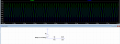
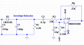
I'm new to the forum. I have a preamp circuit where I am trying to make a demodulator for a LSK circuit(Load-shift-keying or backscattering) and am currentley simulating it in LTspice. The first stage includes an envelope detector which is fed to an amplifier. This is where I have a problem. The envelope detector outputs the envelope which alternates between 4 V and 2 V and then goes into an opamp. Before that I try to put a DC blocking capacitor to remove the DC bias and make it oscillate about 0 V. The envelope signal has a 6.78MHz frequency. But for some reason the voltage waveform at the output of the blocking capacitor always seems to be an amplified version of the input signal. I am using the MAX44280 opamp model that I downloaded from the AD website. I am attaching the schematic and waveform. Any inputs or notions of where I might be going wrong could be helpful. Thank you.
Note: The signal V(n012) is the ED output and V(n013) is the capacitor output.
 

Attachments

KeithWalker

Joined Jul 10, 2017
3,603
You are using a single supply for U1 with the + input biased to 1.8V. The - input will use that as reference. If you want the output waveform to vary about 0V, put the capacitor in series with the output.
 

MisterBill2

Joined Jan 23, 2018
27,159
The high frequency wave form is present because there is nothing to block it. At the very least, a series resistor and a second capacitor.
In order to recover the envelop you need to filter out the carrier. THAT is a basic element of AM receiver design. You can research it under "Envelope detectors"
 

Thread Starter

varun171

Joined Jan 15, 2025
20
You are using a single supply for U1 with the + input biased to 1.8V. The - input will use that as reference. If you want the output waveform to vary about 0V, put the capacitor in series with the output.
I plan on cascading the output of the MAX44280 with another one for more gain. Hence, I do have another capacitor and resistor at the output of the opamp. The problem still persists even with the changes.
 

Thread Starter

varun171

Joined Jan 15, 2025
20
The high frequency wave form is present because there is nothing to block it. At the very least, a series resistor and a second capacitor.
In order to recover the envelop you need to filter out the carrier. THAT is a basic element of AM receiver design. You can research it under "Envelope detectors"
I'm sorry, could you elaborate on your first two sentences. I did read about ED's from here for selecting values of 'bleed resistor' and capacitor. I do not get where in the circuit you want me to add an additional resistor and capacitor.
 

Thread Starter

varun171

Joined Jan 15, 2025
20
Let me make my question more clear. I don't think the problem has anything to do with the opamp yet but more with the previous stage. In the picture below is an sine wave with an offset and a blocking capacitor. The output works as expected as the AC wave now is shifted down around 0 removing the DC bias. I would like the same to happen in my original circuit. I disconnected resistor R3 from the opamp and probe the input and output waveform of the capacitor C3 but it doesnot resemble a signal which has 0 DC bias like the one below. Does the blocking capacitor behaviour not work for AM modulated waves, just a problem somewhere with the simulation or am I understanding something wrong? Thank you for taking the time to make me understand

I have looked into certain posts contaning a similar question to mine but cannot extract a solution for mine.
https://ez.analog.com/design-tools-...or-at-input-of-comparator-and-operational-amp

https://forum.allaboutcircuits.com/threads/dc-offset-in-my-preamplifier-design.152838/
 

Attachments

KeithWalker

Joined Jul 10, 2017
3,603
Let me make my question more clear. I don't think the problem has anything to do with the opamp yet but more with the previous stage. In the picture below is an sine wave with an offset and a blocking capacitor. The output works as expected as the AC wave now is shifted down around 0 removing the DC bias.
In the example circuit that gives the output symmetrically around 0 volts, the op-amp is using a split supply, with the input referenced to 0 volts.
As I stated in post #2, you are using a single supply with the positive input biased to 1.8V, so that is what the signal on the negative input will use as a reference after the blocking capacitor.
 

ericgibbs

Joined Jan 29, 2010
21,390
Hi 171.
When you apply +1.8V to the Non Inverting input of the OPA, the inverting input due to the OPA feedback resistor will pull up to 1.8V.

Adding a capacitor will not remove the 1.8V DC offset at the input of the amplifier

Ideally, you should use a dual power supply for the OPA.

Also, the circuit is unstable and self oscillates.

E
 

MisterBill2

Joined Jan 23, 2018
27,159
Let me make my question more clear. I don't think the problem has anything to do with the opamp yet but more with the previous stage. In the picture below is an sine wave with an offset and a blocking capacitor. The output works as expected as the AC wave now is shifted down around 0 removing the DC bias. I would like the same to happen in my original circuit. I disconnected resistor R3 from the opamp and probe the input and output waveform of the capacitor C3 but it doesnot resemble a signal which has 0 DC bias like the one below. Does the blocking capacitor behaviour not work for AM modulated waves, just a problem somewhere with the simulation or am I understanding something wrong? Thank you for taking the time to make me understand

I have looked into certain posts contaning a similar question to mine but cannot extract a solution for mine.
https://ez.analog.com/design-tools-...or-at-input-of-comparator-and-operational-amp

https://forum.allaboutcircuits.com/threads/dc-offset-in-my-preamplifier-design.152838/
The reason that there is still the high frequency component in the signal is that there is no "low pass filter" in the circuit. THAT is what I was explaining before. The low pass filter is a very old concept, there is a vast amount of information available. It will not change the DC offset but it would remove the high frequency from the waveform.
 

Thread Starter

varun171

Joined Jan 15, 2025
20
Hi 171.
When you apply +1.8V to the Non Inverting input of the OPA, the inverting input due to the OPA feedback resistor will pull up to 1.8V.

Adding a capacitor will not remove the 1.8V DC offset at the input of the amplifier

Ideally, you should use a dual power supply for the OPA.

Also, the circuit is unstable and self oscillates.

E
Hello, Could you elaborate on how you checked the stability of the circuit and self oscillating behaviour? Thank you
 

MisterBill2

Joined Jan 23, 2018
27,159
In the circuit shown in post #15 there is nothing at all, similar to a low-pass filter, between the output side of the diode and the input of the IC amplifier. I do see a "high-pass filter though. This does not address the DC offset issue, but rather the presence of the high frequency signal in what was intended to be an envelope detector scheme.
 

ericgibbs

Joined Jan 29, 2010
21,390
Bill
If you have a problem with the circuit, address it to the TS, not me.!

If you read the posts the OFFSET issue has been identified.

Please stop confusing the thread with pointless posts.
E
 

Thread Starter

varun171

Joined Jan 15, 2025
20
In the circuit shown in post #15 there is nothing at all, similar to a low-pass filter, between the output side of the diode and the input of the IC amplifier. I do see a "high-pass filter though. This does not address the DC offset issue, but rather the presence of the high frequency signal in what was intended to be an envelope detector scheme.
Yes, it is a high pass filter. But the problem I had was not because of that and a mistake in how the opamp was configured.
 
Top