D flip-flop simulation

Thread Starter

Tokatlı

Joined Oct 6, 2026
9
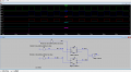
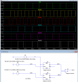
Hi, I'm trying to understand D flip-flop circuits by simulating them in LTspice. I set the CLK signal to a square wave here, but my flip-flop outputs (out1, out2) don't change after 20 ms. Do I need to find a SPICE file for this, or can this issue be resolved using LTspice?
 

Attachments

WBahn

Joined Mar 31, 2012
33,331
Hi, I'm trying to understand D flip-flop circuits by simulating them in LTspice. I set the CLK signal to a square wave here, but my flip-flop outputs (out1, out2) don't change after 20 ms. Do I need to find a SPICE file for this, or can this issue be resolved using LTspice?
Your circuit is doing exactly what you are telling it to do, though the behavior in real life would be erratic.

Consider that happens at 20 ms. You data input goes HI at the same time that the clock signal goes HI. So, what should the output be? Should it be based on the signal just prior to the clock rising edge, or just after? In the real world, flip flops have setup and hold times. The setup is the time before the clock edge at which the data must be established at a valid logic level and the hold time is the time after the edge that it must remain stable. If the data transitions within that window, the final value that is captured is indeterminate. In this case, the simulator is choosing to use the value after it, probably because your data input is 20 V, so it is well above the threshold for a HI at the point that the FF is sampling the signal relative to the clock edge. I you put a 20 V signal into most real FFs, you will be buying new FFs.

Okay, so if we accept the behavior at the first edge, why would that behavior be any different at any other rising edge? So your circuit is just capturing a HI value at every rising clock edge, and hence the output isn't changing.

Change the period of your data, perhaps from 10 ms to 7 ms, and you should see the FFs capturing different data on some of the rising clock edges.
 

eetech00

Joined Jun 8, 2013
4,746
Hi, I'm trying to understand D flip-flop circuits by simulating them in LTspice. I set the CLK signal to a square wave here, but my flip-flop outputs (out1, out2) don't change after 20 ms. Do I need to find a SPICE file for this, or can this issue be resolved using LTspice?
Remove V3 and all connections to "D" pin of each FF.
Then reconnect each "D" pin to its own "Qbar" pin.
 

WBahn

Joined Mar 31, 2012
33,331
Another habit you should get out of the habit of is leaving inputs, such as PRE and CLR, unconnected. YOU need to decide what state those inputs should be at and then YOU need to design your circuit so that they are. Don't let the simulator make your decisions for you. In the real world, especially with CMOS parts, that is a recipe for getting, at best, unexpected behavior and, at worst, parts that have had the magic smoke let out of them. I wish simulators had the ability, at least as an option, to throw an error for unconnected logic inputs. There probably are tools, such as lint checkers, available to analyze the design with that in mind.
 

Reloadron

Joined Jan 15, 2015
7,977
Another habit you should get out of the habit of is leaving inputs, such as PRE and CLR, unconnected.
Very true.

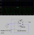
Here is a basic example of a D Flip Flop (CD4013) configured as a /2 flip flop.

CD 4013 D Flip Flop.png

Lower plot is my clock and the upper is my output which is my clock in / 2. Note in this example PRE and CLR are tied to common ground.

Hope that helps a little.

Ron
 

WBahn

Joined Mar 31, 2012
33,331
Did you even try what I suggested? Namely just changing the period of your data from 10 ms to 7 ms?

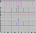
Just making that simple change, despite all of the other issues that have been pointed out, you get:

1792616362413.png

If we slow down the data so that there are multiple clocks per data state, it's even easier to see. Here's what it's like if we change the data signal to a 30 ms period with a 15 ms on-time:
1792616890064.png
 

crutschow

Joined Mar 14, 2008
38,936
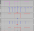
Below is the sim of your circuit with some arbitrary changes to the various signals' timing to get some variety of outputs (and insure that the D and CLK-rise changes are never coincident, which is a no-no), with an OUT3 for the AND gate output:
(Why did you have a V3 voltage of 20V?)

Note that the FF output changes state to whatever the D state is when its CLK signal rises.

1792620159540.png
 
Last edited:

Thread Starter

Tokatlı

Joined Oct 6, 2026
9
Did you even try what I suggested? Namely just changing the period of your data from 10 ms to 7 ms?

Just making that simple change, despite all of the other issues that have been pointed out, you get:

View attachment 372476

If we slow down the data so that there are multiple clocks per data state, it's even easier to see. Here's what it's like if we change the data signal to a 30 ms period with a 15 ms on-time:
View attachment 372477
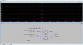
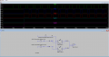
I tried setting the VIN1 period to 12 ms, and it worked—so I actually tried what you suggested—but when I set all three VIN inputs to the same period, as shown in the second image, why does the output stabilize after a certain number of milliseconds? Could you explain this in simple terms?
 

Attachments

Thread Starter

Tokatlı

Joined Oct 6, 2026
9
Below is the sim of your circuit with arbitrary changes to the various signals' timing to get some variety of outputs, and with an OUT3 for the AND gate output:
(Why did you have an IN1 voltage of 20V?)
Note that the FF output changes state to whatever the D state is when the CLK signal rises.

View attachment 372485
This value was assigned to me; it is not a voltage value I chose
 

eetech00

Joined Jun 8, 2013
4,746
I tried setting the VIN1 period to 12 ms, and it worked—so I actually tried what you suggested—but when I set all three VIN inputs to the same period, as shown in the second image, why does the output stabilize after a certain number of milliseconds? Could you explain this in simple terms?
there is “setup time” that’s required.
The D input must be present before the clock pin is “clocked”. Make V3 delay shorter that the clock input signal delay.
 

crutschow

Joined Mar 14, 2008
38,936
why does the output stabilize after a certain number of milliseconds? Could you explain this in simple terms?
It doesn't "stabilize", it's just the output based upon the D input.

Look at the D voltage value just before (not coincident with) the CLK voltage rising.
That determines the output state after the CLK rise.
If the D state is the same as the output state, the output does not change.
If the D state is the opposite of the output state, then the output changes state.

You must set the signal timing parameters such that the D voltage change is never coincident with the CLK voltage rise, otherwise the output will be indeterminant.
 
Last edited:

WBahn

Joined Mar 31, 2012
33,331
I tried setting the VIN1 period to 12 ms, and it worked—so I actually tried what you suggested—but when I set all three VIN inputs to the same period, as shown in the second image, why does the output stabilize after a certain number of milliseconds? Could you explain this in simple terms?
As D Flip Flop captures the state of the data input at the rising edge of the clock. It then holds that state at its output until the next rising edge of the clock, at which point it repeats that process and captures whatever the data input is at that moment. If the data input is changing at that same time, it is indeterminate which state is captured, the state just before the clock edge, or the state just after the clock edge. As stated in Post #2, that is why you don't let the data inputs change at the same time the clock is changing.

Also as stated in Post #2, because you are using unrealistic input voltages for you inputs, at the clock edge the LO-to-HI data transition is already above the threshold at the moment that the clock captures it, so it results in a HI. The flip flop is NOT going HI on the first clock and then "stabilizing", it is getting captured as a new HI on EVERY rising clock edge.
 

schmitt trigger

Joined Jul 12, 2010
2,280
This value was assigned to me; it is not a voltage value I chose
Tell to the person who assigned that voltage value to you, that the magic smoke will come out of the IC right at the very first moment after you power up a real circuit.
If that person balks at the suggestion, ask him to read the “Maximum Ratings” section of the component’s data sheet.
 

WBahn

Joined Mar 31, 2012
33,331
This value was assigned to me; it is not a voltage value I chose
Assigned by who?

Is this a homework assignment of some kind?

What, exactly, is it you are supposed to be doing?

Who came up with the waveforms you are using? Did you? Or were they given in the assignment?
 

WBahn

Joined Mar 31, 2012
33,331
Tell to the person who assigned that voltage value to you, that the magic smoke will come out of the IC right at the very first moment after you power up a real circuit.
If that person balks at the suggestion, ask him to read the “Maximum Ratings” section of the component’s data sheet.
Or, better yet, drop the course, demand a refund, and transfer to a real school.

In fairness, no logic family is specified, so we don't know what the relevant data sheet is. The CD4000 family has an absolute maximum supply voltage rating of 20 V (which people should NOT push). But if that where fine, the sim implies that the chips are being powered by 5 V and so supplying an input signal that is 20 V is almost certainly a big no-no as this will forward bias the protection diodes and, with that kind of voltage difference, almost certainly destroy the part. But, there are chips that are designed to handle higher input voltages than their supply, but these are usually buffers or inverters that are being used to perform level translation. I'm not aware of any flip-flop devices that do this.
 
Top