Cycling between sub-circuits

Thread Starter

NickB

Joined Feb 1, 2016
95
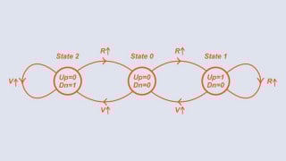
Hi Guys, I have a circuit which currently uses an RF receiver to fire two coils (see schema), using two separate channels on the receiver. I'd like to use only one channel so that it cycles between each coil. For example: activate channel A and it fires coil A, activate channel A again and it fires coil B this time, then back to coil A and so on.

I read somewhere about using a counter chip or something but I've no idea if this would work or if there's an easier solution to incorporating this in my circuit?

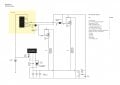
Ignore parts list and blocky nature of schema - that's just for my tiny brain!

Any help greatly appreciated.

Cheers
Nick
 

Attachments

Thread Starter

NickB

Joined Feb 1, 2016
95
You would need 4 states to cycle the possibilities.
example:
00 all off
01
10
11 all on

So yes, a 2-bit binary counter would work but you need to trigger on both the negative and positive going clock (A) edges to get a output state change with every A level change.
https://www.allaboutcircuits.com/worksheets/counters/
Thanks nsaspook, I'm a bit out of my depth here as I'm still a bit of a novice. Any thoughts on how I'd incorporate a counter chip in my circuit?

Kind regards
Nick
 

MrChips

Joined Oct 2, 2009
34,812
I don't see where it is required to have both channels ON and OFF.
Perhaps a simple 555-timer circuit is all that is needed.
 

iONic

Joined Nov 16, 2007
1,662
I agree with MrChips. It also appears that the activation is only momentary to fire a coil. The worst part...one button can not do what he wants. One button can not activate coil A, coil A, Coil B, Coil B unless this is a pre-designed pattern. In other words button 1 can not perform the OR function randomly. I think we need a better explanation of what the op wants.

My bad. I misread his sequencing.

https://circuitdigest.com/electronic-circuits/toggle-switch
 
Last edited:

eetech00

Joined Jun 8, 2013
4,705
Hi

It’s my understanding you want to “toggle”
between the two coils.(?)
What are the coils? Relays?
Do the coils need constant energy when energized? Or pulsed?
What is the required initial state?

eT
 

AnalogKid

Joined Aug 1, 2013
12,130
According to the schematic in post #1, the RX output sets the coil on time. Sticking with that, I think one D flipflop wired as a toggle ff, and two AND gates will work. The RX output pulse goes directly to the ff clock input *and* one input of each AND gate. The ff Q and -Q outputs go to the other AND inputs (1 each). The two AND outputs go to the optos driving the FETs. For extra opto drive current, parallel the two remaining AND gates.

What is the power supply voltage for the coils?

ak
 

Thread Starter

NickB

Joined Feb 1, 2016
95
I agree with MrChips. It also appears that the activation is only momentary to fire a coil. The worst part...one button can not do what he wants. One button can not activate coil A, coil A, Coil B, Coil B unless this is a pre-designed pattern. In other words button 1 can not perform the OR function randomly. I think we need a better explanation of what the op wants.

My bad. I misread his sequencing.

https://circuitdigest.com/electronic-circuits/toggle-switch
Many thanks for the link, I’ll check it out. Sounds like some kind of toggle switch is just what I need.

Regards
Nick
 

Thread Starter

NickB

Joined Feb 1, 2016
95
Hi

It’s my understanding you want to “toggle”
between the two coils.(?)
What are the coils? Relays?
Do the coils need constant energy when energized? Or pulsed?
What is the required initial state?

eT
That’s correct. The coils are electromagnets - each coil just requires a single pulse to fire once. They are used for moving objects.

Regards
Nick
 

Thread Starter

NickB

Joined Feb 1, 2016
95
According to the schematic in post #1, the RX output sets the coil on time. Sticking with that, I think one D flipflop wired as a toggle ff, and two AND gates will work. The RX output pulse goes directly to the ff clock input *and* one input of each AND gate. The ff Q and -Q outputs go to the other AND inputs (1 each). The two AND outputs go to the optos driving the FETs. For extra opto drive current, parallel the two remaining AND gates.

What is the power supply voltage for the coils?

ak
Thanks for the input AK, it sounds interesting but may be beyond my capabilities to visualise. For info, the supply voltage to the coils is approx 240 volts once the cap bank is fully charged.

Regards
Nick
 

eetech00

Joined Jun 8, 2013
4,705
Hi

This is basically what AK has suggested.

I've added a small RC delay to prevent a spike at the "ANDed" outputs that would cause both mosfets to be energized at the same time. If the opto input drive current is higher than about 10 ma, the may each need to be driven by a transistor.

eT

FF Driver Circuit Sim.png
 

Thread Starter

NickB

Joined Feb 1, 2016
95
Hi

This is basically what AK has suggested.

I've added a small RC delay to prevent a spike at the "ANDed" outputs that would cause both mosfets to be energized at the same time. If the opto input drive current is higher than about 10 ma, the may each need to be driven by a transistor.

eT

View attachment 167832
Hi eT

Thanks so much for your input, greatly appreciated and thanks for the schema. Just studying it and looking at the chips involved - I'm seeing 4 x logic gates and 1 x flip flop, is that correct?

Kind regards
Nick
 

AnalogKid

Joined Aug 1, 2013
12,130
Looks good to me. I thought about the spike-suppression, but it could create another kind of spike if the two paralleled gates transition at slightly different voltages. I think the robustness of CMOS can handle it, so this is better than the possible problems of both FETs being on at the same time.

ak
 

AnalogKid

Joined Aug 1, 2013
12,130
Let me expand. First, there is no need for the R5 and R6 resistors. I don't know about you, but in general people put a resistor in series with a MOSFET gate (and not part of a voltage divider) for one of two reasons.

First, they've seen it often in other designs. It comes from the switching power supply world, where the resistor helps dampen a resonant oscillation caused by the package lead and PCB trace inductances and the gate-source capacitance. Back when, it was a surprise to find that a 100 kHz switching power supply failed FCC or MIL-STD-461 emissions testing at 100 *mega* hertz. So people started seeing it in designs without knowing the exact reason, and probably thought it had something to do with reliability/protecting the gate. It doesn't. And in this circuit it is not necessary because the activation signal is not repetitive at or above 10 kHz, and the gate charge is way too small to matter.

Second, it looks weird without them. After years (or decades) of putting a resistor in series with a bipolar transistor's base, it is strange not to have a series resistance going into *any* transistor. But in this application there is no need for them. However, we can use those resistors somewhere else ...

... at those paralleled gate outputs. In high reliability design circles they are a critical design fault. Even though any cross conduction currents would last only a few nanoseconds and be limited by the CMOS transistors' channel resistances, that's not good enough when you're flying to Mars, landing a 747, or embedded in a pacemaker. Each output should have its own current limiting impedance.

So it turns out that there *is* a need for R5 and R6, over there next to R3 and R4. To keep the purists happy, add two more gate resistors so there is one from each gate output to its respective optocoupler. Leave the values at 1.0 K each, to limit the output current per gate to around 4 mA.

ak
 
Last edited:

eetech00

Joined Jun 8, 2013
4,705
Hi eT

Thanks so much for your input, greatly appreciated and thanks for the schema. Just studying it and looking at the chips involved - I'm seeing 4 x logic gates and 1 x flip flop, is that correct?

Kind regards
Nick
Yes. 1ea CD4013B and 1ea CD4081B. Also, not shown, are bypass caps (0.1uf) across the power supply pins of each IC.

Also, along with AK suggestions, I think the opto circuit can be re-configured so that parallel "AND" gates may not be required. Since the mosfets are voltage driven, there doesn't need to be much current transfer by the opto. Rewire the opto so that the opto diode is on and use a load resistor from +5 to the opto transistor collector. Then connect the mosfet gate to the junction of the collector and load resistor. Each opto should sink about 4ma with a 1k current limit resistor.

See alternate circuit below.

FF Driver Circuit Sim2.png
 
Top