Constant current dummy load. Please review & suggest.

Thread Starter

IcedFruits

Joined Jan 15, 2014
97
Made this schematic after being inspired by many youtube videos. Its a bit customized, so, please review and suggest.
So, that's it, I hope nothing will blow up. :)

(Modified schematic as per suggestion received)


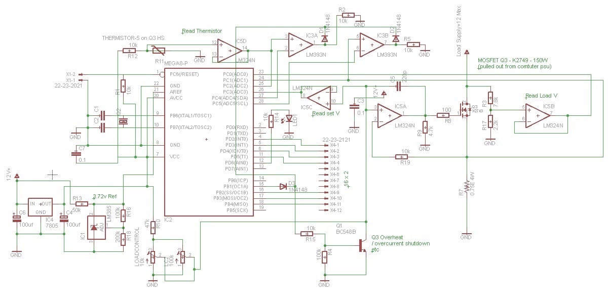
correction: i connected thermistor to +ve in put, but it should go to -ve, as thermistor resistance decrease with temp.
 
Last edited:

ronv

Joined Nov 12, 2008
3,770
There is some missing info to be totally sure so I'm going to guess that your max current is 5 amps. We need to know the maximum voltage of the source supply but I guessed no more than 12 volts. If it's more than that there may be other problems.
So here is what I would do.
Use the 2N7000 to pull the adjustment pot to ground that way you can eliminate the transistor.
Make the load resistors larger so you can read the current directly rather than add another op amp.
This lets you get all the "stuff" out of the feedback path of the op amp so it will be less likely to oscillate.
Just use a divider to read the supply voltage.
I used a lower voltage FET with a higher power rating to try and give more margin.
The FET dissipates 50 watts, so you need a big heat sink that will allow a temperature rise of only about 1C per watt. That should give you a heat sink temperature of about 75C and a junction temperature of the FET at about 125C.
 

Attachments

DickCappels

Joined Aug 21, 2008
10,152
You might find that you will need to reduce the AC gain of IC1A to prevent oscillation and reduce low frequency (flicker) noise on the output of the load.

If you are going to make a PC board, you might want to lay the circuit out to accommodate a resistor in series between the output of IC1B and the inverting input pin of IC1A.

Then you can place negative feedback components between IC1A's output and inverting input.
 

Thread Starter

IcedFruits

Joined Jan 15, 2014
97
What is the maximum current your load can handle?
What is the maximum low-load voltage you load can handle?
I presume it's the voltage of the power supply under test and needs monitoring?

Interesting project. I will keep my eye on this one.
Exactly, and what might be the absolute maximum ratings of the micro-controller?
Load upto 12V / 4A, but wont allow more than 3.3A. & yes, for testing power supplys, rechargeable batteries, including controlled discharge of those batteries.
MC will sense upto 1.1 v (maximum pot voltage is also same) from 1W resistors & 2.2V from test supply.

What kind of voltage do you expect on pin 23?
12V max. Forgot the voltage divider, fixed. (may still change the resistors to 10k & 2.2k pair tho )

Use the 2N7000 to pull the adjustment pot to ground that way you can eliminate the transistor.
Make the load resistors larger so you can read the current directly rather than add another op amp.
This lets you get all the "stuff" out of the feedback path of the op amp so it will be less likely to oscillate.
Just use a divider to read the supply voltage.
I used a lower voltage FET with a higher power rating to try and give more margin.
The FET dissipates 50 watts, so you need a big heat sink that will allow a temperature rise of only about 1C per watt. That should give you a heat sink temperature of about 75C and a junction temperature of the FET at about 125C.
Thanks for all the above suggestions, including the pot grounding one, but how does it eleminate the transistor ? i m supplying 324 with 3.3v. Well, checked ur schematic, 12v supply to lm324. i actually wanted to supply it with ams 1117, since its o/p is more precise and stable. & also because i wanted to power the whole thing with a 9v batt.

so, putting a transistor is a bad idea and will cause oscillation ?

and yah, got a 6cm X 5cm X 5mm heatsink to support the 150W Mosfet. It will dissipate 12X3.3= ~40W at most.

You might find that you will need to reduce the AC gain of IC1A to prevent oscillation and reduce low frequency (flicker) noise on the output of the load.

If you are going to make a PC board, you might want to lay the circuit out to accommodate a resistor in series between the output of IC1B and the inverting input pin of IC1A.

Then you can place negative feedback components between IC1A's output and inverting input.
Trying to decypher the effect of gain thing, u mean to add a resistance between o/p of 1C & i/p(-) of 1A ? cause 1B is just a spare.

Changed the schematic, hope its a bit more clear now.
 
Last edited:

ronv

Joined Nov 12, 2008
3,770
The 324 needs a higher supply voltage than 3.3 volts. The FET may not even start to turn on until it's gate is 4 volts higher than the source and the output of the 324 will only go to about 1.5 volts less than the supply voltage. The 9 volt battery might work ok.
The way the circuit works is that the op amp wants the voltage at the +/- inputs to be the same. So it the pot is set to 1 volt it will try to make the - input the same by increasing the current. The fact that IC1C has gain will make the current much lower than you think. The addition of the transistor and the additional op amp (IC1C) will lower the phase margin and may cause oscillation. I haven't simulated it, but I don't think it is what you want. You will need a much larger heat sink - about 2500 sq. cm of surface area.
 

bance

Joined Aug 11, 2012
315
Other options that might help are:-

  1. use a logic level mos-fet,
  2. utillise the other op-amp and an an additional mos-fet to effectively parallel the current sink.
  3. Drop the value of the sense resistor to lower the source voltage.
HTH Steve.
 

Thread Starter

IcedFruits

Joined Jan 15, 2014
97
@ronv
i am using this st lm324 : http://www.st.com/st-web-ui/static/active/en/resource/technical/document/datasheet/CD00000457.pdf
it operates @3v without problem.
the idea of using BC548B was to drive the 10v gate of mosfet with 1.5v o/p of opmap, as the emitter 10k will be having 0-8.7v for a 9v power supply.

i want to simulate these models in ltspice, but dont have lm358 or 324 there, can you please share the lm358 / 324 files and tell me how to install them ?

2500sq cm = 0.5m X 0.5m u mean half metre by half metre heat sink ! :eek:

the op amp operation issue, i did some miscalculations in schematic, pot max voltage is ~1v, sense resistors max voltage should be 1v too, but i took it as 0.25 as max. i will update the schematic soon, with pot voltage ~2.25v & sesnse resistor max voltage amped to ~2.5v as well.

@bance
thanks for suggestions, will look into them. about lowering the sense resistor voltage, got 4x 1W resistors (1%) , will try to mount them on some metal. but lowering sense resistor voltage too much may give errors, as datasheet says i/p offset voltage of 5mv may occur.
 
Last edited:

ronv

Joined Nov 12, 2008
3,770
@ronv
i am using this st lm324
it operates @3v without problem.
The op amp will work there but the FET may need up to 4 volts just to begin to turn on. Check the gate threshold spec for the FET. You can not get more that the positive supply voltage out of the op amp.

the idea of using BC548B was to drive the 10v gate of mosfet with 1.5v o/p of opmap, as the emitter 10k will be having 0-8.7v for a 9v power supply.
The emitter will be .7 volts less than the base.

i want to simulate these models in ltspice, but dont have lm358 or 324 there, can you please share the lm358 / 324 files and tell me how to install them ?
You can use the LT1013 or 14 from the LTSpice library, it is similar to the 324. I can give you the 324 if you like, but it will be much easier to use the LT1013.

2500sq cm = 0.5m X 0.5m u mean half metre by half metre heat sink ! :eek:
Yes it is a large heat sink, but you can count both sides of the fins so it is not as bad as you might think. Page down in this link for the heat sink calculator.


http://www.tuberadio.com/coils/coil3.html
the op amp operation issue, i did some miscalculations in schematic, pot max voltage is ~1v, sense resistors max voltage should be 1v too, but i took it as 0.25 as max. i will update the schematic soon, with pot voltage ~2.25v & sesnse resistor max voltage amped to ~2.5v as well.
You can use the 3.3 or 5 volts for the pot, but you should use the 9 volts for the power to the op amp.
 

Thread Starter

IcedFruits

Joined Jan 15, 2014
97
ok, understood, i messed up transistor basics. will go read again.

anyways, all those amp ideas in feedback path were because i wanted to lower the effect of opamp offset i/p voltage of 2-5mv, for cases when test current is lowish like 100 - 200mA (sense resistor voltage 25-50mV). now i really want to change the control opamp to some low offset one.

i know OP07 is there that gives very low offest of 0.15uA or less, i will have to visit shop to get that, otherwise, i found one CA3140E in my collection, bought long ago for some long forgotten reason.

as now i am just going supply the opamp with 9-12v, connect the o/p direct to mosfet and eleminate all parts from feedback path, what would be the better IC to use ?

buy OP07 from shop or use my existing CA3140Ewith offset nullification option with trimmpot as written in data sheet ?
 

ronv

Joined Nov 12, 2008
3,770
anyways, all those amp ideas in feedback path were because i wanted to lower the effect of opamp offset i/p voltage of 2-5mv, for cases when test current is lowish like 100 - 200mA (sense resistor voltage 25-50mV). now i really want to change the control opamp to some low offset one.
That's one reason I used a larger resistor for the sense resistor. I was also concerned about running your resistors at full rated power. They will have some change of value causing errors as they heat up.
i know OP07 is there that gives very low offest of 0.15uA or less, i will have to visit shop to get that, otherwise, i found one CA3140E in my collection, bought long ago for some long forgotten reason.
If you can get the LT1014 it has low offset, the input works to ground and the output goes almost to ground.
Actually for the price the 324 is not all that bad if you use the bigger resistor.
 
That's one reason I used a larger resistor for the sense resistor. I was also concerned about running your resistors at full rated power. They will have some change of value causing errors as they heat up.
+1
I'm building one also, hoping for 0-5A, using two mosfets, and a 1Ω resistor bank (12x12Ω 5W) - even running at 40-50% of rated power it gets really hot.... so much that I'm considering a much larger resistor than this....
 

ronv

Joined Nov 12, 2008
3,770
You need to use an op amp for each FET when you put them in parallel like that because they are not operating as a switch so they may not share well.
I've worked with 2 guys on another forum and we've done 50 amp ones - water cooled FETs. :rolleyes:

Here is a smaller one showing how to parallel the FETs.
 

Attachments

Thread Starter

IcedFruits

Joined Jan 15, 2014
97
@ronv
i actually have 10x10E 5W resistors, they are probably 5% or worse (not sure), on the other hand, have some 1E 1W 1% ones, i may look for other resistor options, but let me settle on the op amp first..... i dont think LT components are avilable that easily here, LT & MAX are the last ones they stock here, mostly st/phillips/hitachi/motorola are available, still i will look.
so, i was asking, is CA3140E with offset adjustment trimmer is not as good option as these low offset LT1014/ OP07 ?

& pls share lm324 ltspice files with installation steps, it will be a good and familiar thing to have.

@samuel.whiskers
to much resistance, too much heat, isnt 5x 5E1W better than 12x 12E5W ? :rolleyes:
 

ronv

Joined Nov 12, 2008
3,770
I don't think either of your op amp outputs go to ground which is needed for the low currents.

here are the models for the 358.

Make 2 new folders named new. One in LTC/LTspiceIV/LIB/sub and one in LTC/LTSpiceiV/LIB/sym.
Copy them into something like note pad then
Save the sub file into the new sub folder and name it LM358.sub
LM358.sub is the file name, it should be saved as a text file.

Save the symbol file into the new sym folder and name it LM358.
To add it to your schematic click on the little component symbol look in the new folder and you should find it.


This is the sub file

* LM358 OPERATIONAL AMPLIFIER "MACROMODEL" SUBCIRCUIT
* CREATED USING PARTS RELEASE 4.01 ON 09/08/89 AT 10:54
* (REV N/A) SUPPLY VOLTAGE: +/-5V
* CONNECTIONS: NON-INVERTING INPUT
* | INVERTING INPUT
* | | POSITIVE POWER SUPPLY
* | | | NEGATIVE POWER SUPPLY
* | | | | OUTPUT
* | | | | |
.SUBCKT LM358 1 2 3 4 5
*
C1 11 12 5.544E-12
C2 6 7 20.00E-12
DC 5 53 DX
DE 54 5 DX
DLP 90 91 DX
DLN 92 90 DX
DP 4 3 DX
EGND 99 0 POLY(2) (3,0) (4,0) 0 .5 .5
FB 7 99 POLY(5) VB VC VE VLP VLN 0 15.91E6 -20E6 20E6 20E6 -20E6
GA 6 0 11 12 125.7E-6
GCM 0 6 10 99 7.067E-9
IEE 3 10 DC 10.04E-6
HLIM 90 0 VLIM 1K
Q1 11 2 13 QX
Q2 12 1 14 QX
R2 6 9 100.0E3
RC1 4 11 7.957E3
RC2 4 12 7.957E3
RE1 13 10 2.773E3
RE2 14 10 2.773E3
REE 10 99 19.92E6
RO1 8 5 50
RO2 7 99 50
RP 3 4 30.31E3
VB 9 0 DC 0
VC 3 53 DC 2.100
VE 54 4 DC .6
VLIM 7 8 DC 0
VLP 91 0 DC 40
VLN 0 92 DC 40
.MODEL DX D(IS=800.0E-18)
.MODEL QX PNP(IS=800.0E-18 BF=250)
.ENDS

This is the symbol file.

Version 4
SymbolType CELL
LINE Normal -32 32 32 64
LINE Normal -32 96 32 64
LINE Normal -32 32 -32 96
LINE Normal -28 48 -20 48
LINE Normal -28 80 -20 80
LINE Normal -24 84 -24 76
LINE Normal 0 32 0 48
LINE Normal 0 96 0 80
LINE Normal 4 44 12 44
LINE Normal 8 40 8 48
LINE Normal 4 84 12 84
WINDOW 0 16 32 Left 0
WINDOW 3 16 96 Left 0
SYMATTR Value LM358
SYMATTR Prefix X
SYMATTR SpiceModel New/lm358.sub
SYMATTR Value2 LM358
SYMATTR Description Quad OP Amp
PIN -32 80 NONE 0
PINATTR PinName In+
PINATTR SpiceOrder 1
PIN -32 48 NONE 0
PINATTR PinName In-
PINATTR SpiceOrder 2
PIN 0 32 NONE 0
PINATTR PinName V+
PINATTR SpiceOrder 3
PIN 0 96 NONE 0
PINATTR PinName V-
PINATTR SpiceOrder 4
PIN 32 64 NONE 0
PINATTR PinName OUT
PINATTR SpiceOrder 5
 

DickCappels

Joined Aug 21, 2008
10,152
The common mode input voltage range of the LM324 and LM358 includes ground.

IcedFruits wrote:

"Trying to decypher the effect of gain thing, u mean to add a resistance between o/p of 1C & i/p(-) of 1A ? cause 1B is just a spare."

Yes, you deciphered the message Sorry for the error.


I suggest that you connect the input and local feedback components for IC1A as shown above. The capacitor C1 is not needed. You probably won't need R2, but if it turns out that you need it, it would be far better to already have a place for it on the PC board.
 

Thread Starter

IcedFruits

Joined Jan 15, 2014
97
@ronv
but the opamp's non inverting i/p reaches ground when pot knob is turned down ? effectively the opamp o/p should go to something that makes sense resistor voltage = ground also.....

& thanks for the lm358 codes :)
i have chaged the schematic as per suggestion, please see.

@DickCappels
thanks for suggestion, but some design changes took place. please recheck ! :D
 
Last edited:
Top