Facebook
 Google
 GitHub
 Linkedin
hi Jony, ebp.
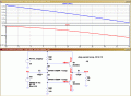
This is LTS sim of the diode temperature range, showing Collector current change with temp.
E
Upper plot trace is -20C
This is LTS sim of the diode temperature range, showing Collector current change with temp.
E
Upper plot trace is -20C
Attachments
-
 29.2 KB Views: 13