Class AB amp with class A driver

Thread Starter

bosko47

Joined Mar 24, 2016
23
I'm trying to get my head around this circuit, the dual power supplies are throwing me off a bit. I need to find component values, showing calculations from a DC and AC viewpoint in order to get a 14dB voltage gain with 20W output power, and greater than 2k input resistance.

Am I correct in saying that Q1 is driving the push-pull configured Q2 and Q3? If I need a 14dB voltage gain (5), would I get that from Q1, since the gain from Q2 and Q3 will be 1. Does this circuit have a particular name? I can't find any examples to help me with understanding the circuit operation.
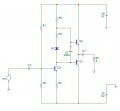
circuit 1.jpg
 

Motanache

Joined Mar 2, 2015
540
I'm waiting with interest for this discussion because it is a very practical problem.

Q2 and Q3 are emitter followers.The output voltage before C2 will be about the same as in the T1 collector.

As voltage amplification we have to calculate a single stage transistor amplifier with the common emitter Q1 transistor.

Q2 and Q3 increase the output power(decrease the output impedance).
 

Jony130

Joined Feb 17, 2009
5,488
Am I correct in saying that Q1 is driving the push-pull configured Q2 and Q3?
Yes, Q1 is a Common Emitter amplifier and provide the voltage gain.

If I need a 14dB voltage gain (5), would I get that from Q1, since the gain from Q2 and Q3 will be 1.
Yes, you are right

Does this circuit have a particular name? I can't find any examples to help me with understanding the circuit operation.
I don't know any.
https://forum.allaboutcircuits.com/...ed-on-push-pull-amplifier.101749/#post-766570

C2 capacitor is not needed if you have split supply in your circuit.

And to get 20W at 8Ω load we need:
VL_max = √(2*Pout*RL) = √(2*20W * 8Ω) ≈ 18V peak
IL_max = VL_max/RL = 2.25A peak

As you can see yor supply is too low. If the output transistors β is equal to 50 the CE stage quiescent current need to be larger then:
Ic1 > IL_max/β = 45mA
 
Last edited:

Thread Starter

bosko47

Joined Mar 24, 2016
23
Thanks Jony for the guidance, but how is the supply too low, if I've got 20v rails and the max peak value is 18v, don't I have 2v to spare?
 

Jony130

Joined Feb 17, 2009
5,488
but how is the supply too low, if I've got 20v rails and the max peak value is 18v, don't I have 2v to spare?
Yes, you have the 2V of headroom. But that's not enough for this type of a circuit.

The maximum positive voltage at the load in this circuit we get when Q1 and Q2 are in cut-off (OFF).
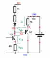
The situation is shown here: (Q1 and Q3 are OFF and I remove the C2 capacitor because is is not needed)

Power_amp1.png

As you can see we can write KVL to find Vo voltage:

Vo = Vcc - Vbe - VR3 = 20V - 0.7V - VR3

So if we want Vo = 18V then the voltage across VR3 is equal to:

VR4 = 20V - 0.7V - 18V = 1.3V

And what about IR3 ??
We need 2.25A of current into the load. The Q2 current gain is β = 50, so, the Q2 base current need to be Ib2 = IR3 = Ie/(β + 1) = 2.25A/51 = 44.2mA

Therefore the R3 value is :

R3 = 1.3V/44.2mA ≈ 27Ω

As you can see R3 need to have a very low value, additional without the input signal the IR3 current will be much larger than this 44mA.
For exampel without the signal the R3 curren will be around 20V/27Ω = 0.74A and this is the Ic1 collector current also.

The situation for maximum negative voltage is also not good with such a low headroom voltage.

This time Q2 is OFF

Power_amp2.png

This time we have additional Q1 Vce saturation voltage, but we still have VR5 and Vbe3. So, the situation looks worse.

Do you understand any of this? Because I'm only scratch the surface here.
 

Jony130

Joined Feb 17, 2009
5,488
In practice, do you think it is a good idea to use Darlington transistors for Q2 and Q3?
Yes, you can use the Darlington or the complementary version (NPN/PNP) the Sziklai pair
http://1.bp.blogspot.com/-5t0y2KuHQt4/Vnb7Hk2RedI/AAAAAAAABww/GxAonBlvl0c/s1600/sziklai_pairs.png

Can you tell me once again the difference between β and hfe?

I'm interested in how we can use to solve this problem, If we find in the datasheet only Hfe or hfe and not β ?
The β is a BJT current gain for DC

β = Ic/Ib and in datasheet DC current gain is HFE

For the AC current the current gain is defined as hfe = ic/ib = ΔIc/ΔIb at constant Vce (vce = 0V)
The Capital letters (Uppercase) represent the DC, and lowercase (v,i) for (small) AC signals.

And because in real life Hfe (β) varies a lot from transistor to transistor even the same type or lot (same batch from the factory). Hfe also change with the Ic and temperature. We typically pick the minimum Hfe value from the datasheet and use this in hand calculations.
 
Last edited:
Top