Clap switch with latching relay

Parkera

Joined May 3, 2016
127
Hi Copey84 – glad to see you are gaining a good understanding of the circuit and your test equipment, as well as an appreciation of through up-front testing of any circuit.

Recognize that the comparator output will only go high when the voltage across C2 is above the threshold set by R6 and R7 (1.33 volts). The voltage across C2 will quickly increase to the peak output of U1 minus the forward voltage drop across D1 (~0.6 volts). A loud “clap” will charge to a higher voltage than a quiet “clap”, so you will see some differences each time. Once C2 is charged, it will discharge at a slower rate determined by the value of R5 and C2 time constant.

As soon as C2 is above 1.33 volts, the output of the comparator will go high. C2 immediately begins to discharge slowly, but as long as its voltage is above 1.33 volts, the comparator output will remain high. With a single "clap", the pulse width out of the comparator will be about 0.569 seconds (nominally).
upload_2017-7-28_23-0-46.png
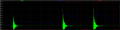
The red trace is the "clap" output of U1. The blue trace is the voltage across C2 (you can't look at it without loading the circuit, but the simulator can). The green trace is the pulse width output of the comparator. Notice that the trailing edge occurs when C2 discharges to 1.33 volts.

Here is what will happen if you clap a 2nd time, say 0.2 seconds later. Just prior to the 2nd clap, C2 will have discharged only to about 2.1 volts. Since this is above the 1.33 volt threshold, the comparator output is still high. When the 2nd clap occurs (at 0.2 seconds), C2 will again charge to the peak output of U1. And it will immediately begin to discharge again. The comparator output will continue to remain high until C2 discharges to 1.33 volts, at which time the comparator output goes low.
upload_2017-7-28_23-20-43.png
You can see that C2 charges to the peak, begins to discharge and is recharged to the peak again when the 2nd clap occurs. Notice that the total pulse width is now 0.769 seconds. It is exactly 0.2 seconds longer than the pulse width caused by a single “clap”. The pulse has been “stretched” by the amount of time in between “claps”. It is still a single pulse out of the comparator, albeit a bit longer. Time between claps up to about 0.5 second will extend a single pulse. Beyond that time, C2 will be able to discharge below 1.33 volts, thus ending the single pulse and a new 2nd pulse will begin. That is why you saw two separate output pulses.

Go ahead and experiment with clapping twice, but spacing the amount of time between claps. Look at the output of U1 and of U2 simultaneously (trust that C2 is discharging like the simulation shows). Trigger on the output of U1, about 1.75 volts.

You should be able to measure quite accurately what the clap spacing time is by looking at the time between the rising edge of the two claps (output of U1). You can measure the single-clap pulse width by measuring the time from the 2nd clap at U1 to the trailing edge of U2 output.

Let me know when you are ready for the rest of the circuit.
 

Parkera

Joined May 3, 2016
127
Hi Copey84 – So now we have a nice, clean and predictable pulse every time you “clap”. Unfortunately, if you were to drive the light directly out of the comparator, it won’t keep a light on for more than a fraction of a second. Therefore, some means of keeping the light on after the pulse must be devised.

There are several circuits that could be used. Electro-mechanical latching relays would be one way, but there are few to choose from. A review of available types in Digi-Key shows that none are capable of switching a 15A lighting circuit, which limits it usefulness. They also require 2 driver circuits and cost about twice as much as a conventional relay that is capable of switching the full 15A lighting circuit.

A better way would be to use digital logic ICs to accomplish the latching requirement. We need a circuit that will change states as soon as the output of the comparator goes from low to high, in other words, we need an edge triggered latching circuit. The most straight-forward latch circuit would be a JK Flip-Flop such as the CD4027. The J and K inputs are set up with permanent “1’s” and the S and R inputs would be set up with permanent “0’s”. By connecting the comparator output (U2) to the clock input, the Q output would only change states (0 to 1 or 1 to 0) when the comparator output switches from low to high.

You started this thread with an interesting circuit based on the CD4017 decade counter. In this circuit, the first clock pulse (comparator output pulse) causes output #1 to go high and remain high until the next clock pulse occurs. This causes output #1 to go low and output #2 to go high. By looping the #2 output back to the reset input, as soon the #2 output goes high, the counter is reset and all outputs go low, accomplishing the same function as the JK Flip-Flop described above. It too is an edge-triggered latching circuit. Since you already have a CD4017 and I have a Spice model for it; we will use that circuit.

Next, the power switching device needs to be selected. Since the lamp is mains powered, it must switch 220V AC, and preferably be rated at 15A. This pretty much limits you to either a triac or a relay. A triac has the advantages of being a solid state device, therefore silent with an essentially unlimited lifetime and a lower cost than a relay. A relay can have a life expectancy of over 100,000 switching cycles and, while not virtually silent, does not make an objectionable amount of noise for this application. Its biggest advantage over a triac is it provides safety isolation of the control circuit from the mains. Omron makes a nice PCB-mounted power relay rated at 250V, 15A with quick-connect terminals for the switched contacts, therefore keeping the mains completely off of a circuit board, easing its spacing requirements. It is available with a 5VDC, 40mA coil. http://www.omron.com/ecb/products/pdf/en-g5ca.pdf. The cost from Digi-Key is $5.12.

The last thing to design is the relay driver circuit (see the complete circuit below). Since the relay has a modest 40mA coil, it can be driven with a common NPN transistor such as a BC547. Using the above relay as a design example, the collector current will be 40mA. The BC547A has an estimated minimum beta of about 90 at 40mA collector current. That means the required minimum base current (Ib) is 0.44mA. The Vbe in full saturation is specified at 0.7 volts. R9 is added to assure a more positive turn-off. A typical value is 2.2K, which will require an additional 0.32mA which we call bias current, to be sourced from U3. The total current through R8 will be 0.44mA + 0.32mA = 0.76mA. U3 source voltage is 5 volts in the high state. R8 can be calculated as (Vu3 – Vbe) / (Ib + Ibias) = (5 – 0.7) / (0.44e-3 + 0.32e-3) = 5.6K. (Note, the circuit diagram shows a 6.2K, not a 5.6K resistor.) Use the 5.6K resistor. Because a relay coil is essentially an inductor, you have to include a diode across the coil in order to suppress the inductive kick voltage. D3 is not a particularly critical type, only needing to handle 5 volts and 40 ma of current. It could also be a 1N4000 series diode. Physically mount the diode as close to the coil as possible.

Below is the complete circuit. The relay coil is simulated by L1, arbitrarily assigned a 100mH inductance. In order to for me to use the model of U3, I had to change "+5" to "Vdd". This is strictly a label change for simulation purposes and is not an electrical change from previous versions of the circuit; everything is still powered by 5 volts..
upload_2017-7-31_20-4-26.png

Below are key waveforms showing the basic operation. The green trace is the output of U3, which, timing-wise is identical to what the light would do. The blue trace is the output of the comparator (U2). The red trace is the output of U1, the analog "clap" signal. In order to show the full cycles on one screen, the timing between "claps" has been kept to 1 second.

The sequence is as follows:
  • There is a short delay of about 50 ms to show initial conditions of the circuit.
  • A single "clap" is picked up by the microphone and is amplified and level shifted by U1 (red trace). The comparator creates a single pulse, approximately 570 ms wide (blue trace), which latches the output of U3 high (green trace), turning on the light. The light remains on until the 2nd "clap" occurs, about 1.05 seconds from the beginning of the simulation.
  • At 1.05 seconds, a second single "clap" is picked up by the microphone, creating a 2nd 570 ms pulse from U2. This causes the output of U3 to be reset into the low condition, which turns off the light.
  • This sequence cycle is performed a 2nd time beginning at 2.05 seconds, which cycles the light on and off again.
upload_2017-7-31_20-23-5.png

The relay driver circuit is pretty basic and doesn't need much further explanation. If you have another preferred choice of relay, it should be OK. Just check the maximum current the relay requires and make sure the transistor can easily handle it, otherwise heat sinking may be necessary. The same goes for the transistor. While I have chosen an NPN bipolar, a JFET or MOSFET could also be used, but they don't gain you anything and are slightly less robust than a bipolar.

Well, that is the whole circuit. As for operation, the circuit is sensitive to sound level, not the timbre of sound. This means that ANY loud enough sound will trigger the circuit. You could even say "lights", and it will work. That is not necessarily a bad thing, just something to be aware of. That is why, early on I wanted to know about the room environment, background noise, etc.

Have fun with it and good luck.
 

Attachments

Last edited:

Thread Starter

Copey84

Joined Jul 27, 2015
198
Hi Parkera, I had a relay coil ordered few months ago that I think will do.
Even though it's only rated for 2A @ 250v AC, with the led lighting load being in miliamps range I think it should be ok.

There's no coil current data but I know the resistance of coil is 178ohms, so 5v/178ohms = 28ma.
I'll check current with meter to make sure but should be ok to use bc547.

Also would you recommend connecting small value caps across both ICs to keep voltage levels stable?
 

Parkera

Joined May 3, 2016
127
Hi Copey84 - The BC547 should handle that relay with no problem.

As for the bypass caps - ALWAYS use them. (Most engineers won't spec them in the breadboard stage, but it is understood to always use them. That was one of the first things I learned on the job after I got out of school.) It is best to put one right at the IC, with the ground lead getting the physical priority. Bring the V+ to the cap, then from the cap to the IC. Typical values are either a 0.01uF or a 0.1uF. They should be a ceramic type capacitor. Use the 0.1uF if you have the space and budget. A 10uF shunted by a 0.1uF at the power supply input to the board should be plenty for this application.
 

Thread Starter

Copey84

Joined Jul 27, 2015
198
Hi Parkera, I connected 4017 ic but it isn't working. Just stuck a 10k resistor and led temporarily between 5v to collector, expected it to plus but nothing.
I think ic pins are correct 16 - 5v
15 - reset connect to pin 2
14 - clock, from U1
13 - clock inhibit to ground
1 - output
8 - ground

Just remembered my relay has two separate coils so I can't really use this set up.
Might have to use original set up with both outputs 1 and 2 connected to separate cap and resistors to create a differentiator circuit that will pulse the two coils.
Is this a suitable way or is there a better way to build it?
 

Parkera

Joined May 3, 2016
127
Hi Copey84 - For troubleshooting, "Divide-and-Conquer" is the most efficient way. You have a valid input (the sound of a "clap"), but no output (the relay doesn't respond). I would look at the 4017 and not initially worry about the relay or driver. I believe you have wiring errors caused by a misunderstanding of the IC pin names. The functions are labeled on the schematic, not the pin numbers. This confusion often happens when working with digital circuits because many of the functions are best described with numbers. Pin numbers can vary, depending on the IC package that is ultimately chosen.
upload_2017-8-2_9-16-35.png
The reset line (pin 15) should be connected to Output "2" (pin 4). The output of the circuit (as shown) is Output "1" (pin 2). The clock input (pin 14) comes from the comparator output, U2 (not U1). Supply, ground and Clock Enable are correct.

Correct the wiring errors and look at U3-Output 1 (pin 2) with the scope; it should mimic what the lamp will ultimately do.

I have never worked with a latching relay, so I don't have direct experience. If you can point me to the data sheet for the relay you have I will give it some thought. But to answer your question "Is this a suitable way or is there a better way to build it?" For starters, a dual-coil relay will require 2 driver circuits at the very least and the pulses required to activate the relay are likely defined and circuitry has to be added/changed to accommodate those requirements. After getting into it, you may find other "gremlins" to be solved. I would just buy a conventional relay and keep life simple.
 

Thread Starter

Copey84

Joined Jul 27, 2015
198
Corrected mistakes and got circuit working.
Had connection to U2, it was others that were wrong.

The reason I wanted to use a latching relay was so I could switch lights on and off without having to keep coil energised. And as I'm going to use relay switch contacts to make a two way light circuit from wall switch it could be on for long periods of time depending on the switch configuration.

Could I use both pins 1 and 2 to feed two transistors with separate caps and resistors to create a pulse at either coil.
Had it setup before and seemed to work ok, but not sure if it's a good solution.

41bn+rZdFNL.jpg
Can't get link to Amazon where I got the relay, but was able to get the pic above.
 

Attachments

Parkera

Joined May 3, 2016
127
Hi Copey84 - I found the data sheet for the relay. (http://www.te.com/commerce/Document...EnglishENG_SS_108-98002_W_P2.pdf5-1393788-8) It really is not a good choice of relay for the application - you can make it work, at least for a while, but it is a poor choice. This relay should be driven by a square wave pulse, at least 30 ms wide, so do not use a differentiator circuit to drive them. This particular relay is designed for controlling low-level signal type applications such as telephone switching, audio and digital signal applications. It is NOT designed for switching mains loads. Contact ratings drop to 250 ma for 240 VAC applications (not 2 amps). Even with an LED light as a load, you would be pushing the limits for the contacts. I STRONGLY RECOMMEND AGAINST USING IT.

Your reason for not wanting the coil energized all the time is no longer valid since you are not trying to use a 9V battery to power it. Conventional relays are designed for continuous use applications. Since you are running the circuit from a wall wort, there is no reason you can't have the relay energized all the time. A relay with "Form C" contacts (single-pole, double-throw) will work just fine in a 3-way light circuit.

My recommendation of using a conventional relay still stands.
 

Thread Starter

Copey84

Joined Jul 27, 2015
198
Hi Parkera, best thing to do is order a new relay.
Checked rs components in UK and seen a conventional Panasonic that suits my spec, going to order today.

I think that's finally everything covered, although there's probably something I've forgotten.

Anyway I can't thank you enough for all your help, must be best instructional guide to build a clapper on internet. Seriously the detail and effort you put in was brilliant, I thank you again and good luck.
 

Parkera

Joined May 3, 2016
127
Hi Copey84 - Thanks for the complements. I have learned a lot over the years and now that I am retired, it is time to pass on the knowledge to the next person; otherwise it is lost for ever. I've enjoyed working on this project with you and it caused me to learn more about electret microphones, latching relays and LT Spice, the simulator program I am trying to learn.

Once you build the final circuit and "install" it into the room, you may find that some tweaking would be desirable. A guide to this tweaking is as follows:
  • If you find the overall sensitivity is either too high or too low - Adjust R4 as required. This is the 'gain' resistor.
  • If you find that the general background noise level is higher than anticipated - Adjust R7 upward. Do this AFTER R4 is adjusted (if you adjust R4). It is not likely that you would need to lower the value of R7, as that would increase the possibility of false triggering from background noise.
  • While it is not likely you would need to change it, C2 adjusts the amount of time that must pass before the circuit is ready to "change states".
    • As you try to increase the amount of time, limits will be reached as determined by available and suitable timing-grade capacitors, input bias current of the LM358, inherent circuit noise causing erratic switching behaviour and general circuit leakage paths. In practice, about the maximum time would be something around 1 minute.
    • As you try to decrease the amount of time, the circuit will actually start to respond to the individual low-frequency components of the "clap" waveform and/or low-frequency room noise. Obviously this translates into false triggering. In practice, about the minimum time would be something around 50 ms to 75 ms.
If you have forgotten anything, just ask. I'll do my best to give you an answer. Good luck with the final build and let me know how it works out.
 

Thread Starter

Copey84

Joined Jul 27, 2015
198
Hi Parkera, that list may come in useful once I've tested breadboarded circuit out in room.
Think I'll leave it setup for a few days and see how it responds to claps and other noises, hopefully not to many false triggers.

Everything I need is on workbench now apart from relay which should be here early next week.
Next step is to sketch out PCB trace and etch it, then put it all together.

I'll let you know how I get on, thanks again.
 

Thread Starter

Copey84

Joined Jul 27, 2015
198
Hi Parkera, I'm back again. I've got a few issues with circuit set up in room of use.
Although there's no false triggers from door opening and closing it does need a loud clap to operate.
I tried increasing R4 to 51k thinking it will increase amplification by reducing feedback, but it hasn't made any difference.
When up closer to mic it operates with a quieter clap, as expected. Could having mic closer to trigger point be a solution instead of changing R4. I'm thinking any changes to R4 may start door false triggering again.

Also when circuit is triggered the led sometimes turns on and off with just one clap. Think the reason for this is because of room acoustics. Certain claps create more of an echo than others, so I'm thinking you get an added spike that turns led off after initial on signal.
I thought increasing C2 may stop the rapid on off so I added another 0.47uf cap in parallel but no change.
Just to note I had to parallel caps as 0.47uf is largest I have.

As I'm writing this I had another few goes at clapping and it is quite inconsistent, kinda as before which is a shame after all effort put in. I know it's impossible to get this circuit working perfectly every time, so I understand there might not really be much more can be done.
Anyway let me know if there's anything else worth trying, thanks.
 
Last edited:

Parkera

Joined May 3, 2016
127
Hi Copey84 – You have made many observations and asked many questions, all kind of inter-twined (not your fault, just the way it really is). I’ll try to sort it out for you the best I can. By “speaker”, I assume you really mean microphone.

First, it’s no surprise that the circuit responds differently in a different room. Acoustics does play a MAJOR role in how the circuit acts. And yes, there is just so much that you can do with a simple circuit such as this.

As I recall, your workshop was relatively small, perhaps 1/3 the volume of your bedroom. About the best you could do was to get the microphone about 1 meter away in the workshop, and it will be about 3 meters away in the bedroom.
  • · While there will be a longer echo time in a larger room, the difference in time between the two rooms will be in the order of 100 ms or so (you actually could measure it with your scope if you really want to). Since the “re-arming time” with a 0.47uF is 570 ms, I wouldn’t think echoes would do anything except extend the “single-clap” pulse width out of U2, as was shown in post #101. As you noted, doubling the 0.47uF (which would make the “re-arming time” 1.14 second) didn’t do anything, which supports looking elsewhere for the solution.
  • The increased microphone distance makes the signal picked up by the microphone in the bedroom roughly 1/10 of what it was in the workshop. Increasing R4 by 8% basically does nothing (which you observed). To be a meaningful change in gain, R4 should be perhaps 470K. This is not necessarily a recommended value, but to give you an idea of how much change is needed.
  • When the gain is increased, unfortunately, all other sounds in the room will also be amplified by the same amount, including background noise, echo signals and door closures. This raises the “noise floor”, but as long as this noise floor is below the comparator threshold voltage, the dynamic range of the circuit hasn’t changed.
The inconsistency you observe is most likely caused by the inconsistency of your “claps”, specifically the peak level of the clap. This is very normal and just about impossible to control with any repeatability. When there is an ample signal from the microphone, the circuit handles this variability is by letting U1 go into saturation on very loud claps, which only extends the point where C2 can begin to discharge (which only extends the pulse width of U2). With a weaker microphone signal (further away from the clap), C2 never reaches a full charge. If that level is below roughly 1.9 volts, U2 will never create a trigger for U3. (1.3 volt threshold + 0.6V drop across D1 = 1.9 volts.)

This is an example of 2 claps, the first is too weak to cause a trigger, followed by a 2nd clap, also marginal but high enough to initiate a trigger pulse from U2. Notice the voltages on C2 (blue trace); the first reaches ~1.2 volts, the 2nd reaches ~2.1 volts.
upload_2017-8-5_23-57-4.png

In the end, moving the microphone closer to the “clap” would certainly solve the problem (but let’s see if it can be solved with the preferred placement first). But instead of using a long cable on the microphone element (which is sensitive to EMI), I would extend the wire going to the light, which does not have ANY sensitivity to EMI.
 

Attachments

Thread Starter

Copey84

Joined Jul 27, 2015
198
Hi Parkera, I tried the 470k but as suspected it made the circuit to sensitive.
Went to a 100k and although better it still needs a loud clap to operate.

The only option is to move the mic as the rest of cables can't be accessed from anywhere else.
If I use a screened cable with mic plug and socket used at circuit housing will this be suitable?
 

Parkera

Joined May 3, 2016
127
Hi Copey84 - Sorry for the delay, our antique car was used in a film so that has kept me busy.

I'm really not to surprised that increasing the gain 10X made the circuit too sensitive. I would have guessed that 220k or possibly a 330k would be the practical upper limit, but even that may still require a fairly loud clap to work well. Try those values and see if you get acceptable results. If not, then bringing the mic closer is probably your best bet.

Definitely use a shielded (screened) cable. If you keep R1 on the PC board, a single-conductor + shield cable is fine. You don't need to match impedances like you do in RF, so you can use just about any kind of shielded cable. You don't need a heavy conductor gauge either, #24 is fine unless you need it for physical durability reasons. If you have the choice, use a braided shield as opposed to a spiral-wrapped shield; it's shielding properties are a bit better, but it does cost more. Because the microphone is the 1st item in an amplifying signal chain, any electrical noise picked up by the leads is also amplified. For this reason it is considered a "sensitive" part of the circuit (although no where near as sensitive as C2). Keep this in mind when laying out the circuit.

Good luck and let me know how it works out for you.
 

Thread Starter

Copey84

Joined Jul 27, 2015
198
Hi Parkera, I moved the circuit to where I will eventually fit the mic on its own.
I've tested it out over past few days with a 100k ohm resistor in place at R4 and it seems to be working ok.
Got it so close to trigger position that a click of the fingers is sometimes all that is needed for operation, although it does still need a clap depending on how much snap I can get in the fingers, sounds silly I know.

Anyway I've finally got to designing the PCB, before I etch it out I just wanted to check about position of C2.
The traces leading up to and especially to ground are short. But my power rail is going to be close, say max distance 5mm and with lots of components around lm358 it's hard to keep much distance.
What would be recommended distance for C2 from other components and power rails?
 

Parkera

Joined May 3, 2016
127
Hi Copey84 – The amount of “snap” doesn’t sound silly at all, just like some “claps” work under a given set of conditions and other times it doesn’t work. Acoustics doesn’t always make logical sense until you know the subtleties of the science. Speaking of which, things may change some too when you put the whole thing in an enclosure and even which way it is facing, once in an enclosure.

Since you have it working much better with a 100K, but not necessarily consistent yet, you may want to consider making R4 a panel pot, perhaps a 250K, possibly with a 22K to 47K resistor in series. (No sense wasting rotation degrees when you know you will need a minimum value anyway.) That will give you the ability to make sensitivity changes if needed, depending on the activity in the room.

Using a panel pot as a feedback resistor is considered poor practice for several reasons, but it is so convenient at times that it is done in non-critical applications. When you do use a panel pot, you want the wiper, which internally is in close proximity to the shaft and mounting bushing, to go to the lowest impedance point, which in this case is the output of U1. The 47K should have one end close to U1 inverting input. The leads to the pot should be twisted together to cancel out any pickup.

Now, a few generic words on layout. Any schematic diagram of a “product” only includes the electrical components which make the circuit work; the purchased components if you will. What is not shown are all of the parasitic components. These are the resistance, capacitance and inductance components of every part, wire, PCB trace, etc. that physically make up the product. Simply, each conductor has the parasitic components of resistance (pretty straight forward), inductance (even a straight piece of wire has an inductance associated with it), a ‘self-capacitance’ which is the capacitance between any two points of the part itself (think the capacitance between turns of an inductor) and the capacitance between any 2 conductors. You want to minimize as much as possible these parasitic components through layout of the circuit.

As you might well imagine, if you were to actually draw out all of these parasitic components and add them to the schematic, it would become an unreadable nightmare. That is where the art and skill of laying out the PCB comes – you have to keep these parasitic components in your head. You have to constantly be thinking of what relationship exists between each other part in proximity (either physical or electrical) as you lay out parts and run traces. You will never remove parasitics, but you can minimize the ones that will have the most impact on the circuit operation. Fortunately in this circuit, any practical amount of parasitic capacitance won’t have much effect at all on the circuit. Practically, parasitic inductance also has minimal impact on this circuit. U3 has the most sensitivity to parasitic inductance, but probably not enough to really worry about (it would slow the rise and fall times). But resistance is another story.

I have found that the key to keeping these parasitics under control is to keep in mind where and how the currents flow in the circuit. For example, the current for C2 starts at the + terminal of the power supply, travels through traces until it gets to the Vdd pin of U1. Exits the output of U1, flows through D1, and places an electrostatic charge on the upper plate of C2. Because this current is ‘changing’ during the charging of C2, there will be a changing current flow through the dielectric of C2, out of the bottom plate, through the ground traces and back to the power supply – terminal. Note: this is ONLY the charging current affecting C2. This total path of the current can be thought of as a series circuit.

At various points in the path there may be additional current flows from other components. For example, the output pin of U1 also supplies the feedback current through R4, which also includes the (additional) input current of the inverting input transistor of U1. U1 output also supplies the input current for the non-inverting pin of U2.

Every current path can be represented as a capacitor shunting a resistor in series with an inductor, to some other point. These “impedances” may be either in series or shunt. Any “series impedance” should be as low as possible to minimize the effect on the circuit and any “shunt impedance” should be as high as possible to minimize the effect on the circuit. Speaking in general rules of thumb, for non-critical circuits such as this “clapper”, if the parasitic elements are under 0.1% of the nominal circuit impedance (resistance), the effect can probably be ignored. If the parasitic elements are over 1% of the nominal impedance, it should be considered a “critical” circuit.

Your head is probably spinning now, but what does all this mean in practice? Every circuit is different but –
  • You should try to minimize the AREA of any current loop. It forms a loop antenna which can both radiate signals and be influenced by external fields. The higher the current flow, the more it radiates. The lower the current flow, the more it will be influenced by external fields. High impedance circuits tend to be impacted more by external fields. Low impedance circuits tend to be less sensitive to external fields, but they will radiate more energy (causing more interference). Be aware that the interference may be to another part of your circuit, setting up oscillation and/or instability or just really bazar operation.
The highest current in this circuit are the relay coil current loops. (Remember, there is also a current flow through D3 when the coil is de-energized.) The C2 charging circuit is probably the next highest, which includes the supply pins to the opamp. Any digital chip also has momentary current spikes, which is why the bypass capacitors are always kept close.​
  • You should try to minimize any series resistance in a current loop. The resistance will create a voltage drop in the circuit, which depending on the circuit, could have different effects. Probably the easiest way to illustrate the problem is through an example. I’ll make the example extreme so it is easier to see what is happening. Let’s change the value of R6 to 3.3 ohms and the value of R7 to 1.2 ohms. Since they are merely scaled, the threshold voltage on U2 will not change (1.33 volts), but the current flow through the divider went from 11.1uA to 1.11A. Now let’s say the return from R7 back to ground is fairly thin (0.5mm) and about 15 cm long. It will have a resistance of 0.145 ohms. This resistance is directly in series to the resistance of R7, effectively making R7 1.345 ohms. This increased resistance will change the threshold voltage from 1.33 volts to 1.45 volts. A useful tool can be found at https://www.eeweb.com/toolbox/trace-resistance.
Whenever you consider the series resistance in a layout, think of the PEAK current levels, not so much the average current level. (In power circuits you have to consider the peak and RMS currents.) In practical track width terms, the L1 to power supply path is all you really have to even think about.​
  • You should keep any components (usually only one end) connected to the NODE really close together. High impedance nodes are susceptible to outside field pickup and the conductors form little monopole-type antennas. If there is a conflict in space, give the high impedance node the priority. “Guard Rings” can sometimes be used around critical nodes, but I don’t think you have to go that far for this circuit.
C2 is critical not only because there are (relatively) high current spikes while it is being charged, but it ALSO becomes a high impedance node when D1 becomes reverse biased. The reason a guard ring is not required is because U2 is not a FET-input opamp and the circuit is not a critical “instrumentation” type circuit. Also, the AC impedance is low due to the reactance of a 0.47uF capacitor within the audio band of frequencies (less than 10K ohms). Yes, you have to think both in terms of DC operation and in the AC & transient operation of the circuit.​
  • Perhaps the most important lesson to learn in laying out PC boards is to use what is known as “STAR” power supply distribution. The purpose is to prevent “ground loops”. Ground loops occur when an inevitable voltage drop caused by wiring parasitics sets up a feedback node (like an opamp) with another circuit.
Star wiring gets its name because the ground from each circuit has a direct run, with no branches, back to the power supply bypass capacitor(s) ground terminal. Each ‘run’ forms the point of a star. In practice, there is usually one main “star”, with each point going to the center of a secondary “star” or sub-star. Each stage has its own star wiring scheme with the bypass capacitors forming the center of the star.

The best way to illustrate this is by re-drawing the schematic. It’s harder to read as a schematic, but the point is to show stage separation, power supply distribution and ground distribution. The GROUND circuit has been highlighted in yellow.​

  • Notice I have added space between stages to separate the stages; microphone, U1/C2, the comparator (U2), digital logic (U3), relay driver (Q1, L1) and the power supply.
  • Notice that there are several lines running back to the power supply bypass capacitors. These are the points of the main star.
  • There are several sub-stars. These are:
    • Q1,R9
    • U3 CLK_INH, U3 ground pin and its bypass
    • U1 and U2 – this is internal to an LM358, and its bypass
    • U2 and R7 (going to the LM358 bypass)
    • U1 and C2 (going directly to the LM358 supply pin. In reality, the LM358 bypass will be physically close to the LM358 – pin (pin 4)
    • R3 and the Mic ground
      • This sub-star connects to the LM358 sub-star
  • Notice similar “sub stars” also exist on the +5 lines to each stage
The microphone +5 has its own run back to the power supply. This is because any noise on it will be amplified by U1, which we don’t want. The mic ground is not brought out separately because we need it to be referenced to the amplifier, U1. If we were to bring a separate line back to the power supply, a ground loop would be set up within the other stages.​

upload_2017-8-10_12-6-51.png
You will notice with all this, the end effect is to isolate each stage from each other except for the actual signal we want to pass between stages. Any high currents go DIRECTLY to the power supply so they can’t impose a changing signal (due to voltage drop) on any other stage (relay circuit). Notice that all references within a stage are isolated with their own star
  • U3 Clock Inh to U3 ground.
  • Comparator reference with the comparator IC (at the bypass)
  • The microphone signal with the amplifier (U1) (Mic, U3, LM358 ground)
  • The amplifier with the offset voltage to partially clip the bottom-half of the waveform (R3, LM358 ground)
  • The charging of C2 (C2, LM358 ground)
Much more could be said on the subject, but there is plenty here for you to digest. Besides, at some point I have to answer your question. It is not a simple answer based on distance alone, it is really about how currents flow (either conducted or “injected”) in the circuit. These are not hard, fast rules that cannot be broken, but guidelines. There are PLENTY of products out there that have horrible PCB layouts, yet the work good enough. I have found that a good circuit will work better with a good layout, and work poorly with a bad layout. This circuit is really not all that critical and it will work OK even with a bad layout. But it will be a little bit more ‘positive’ with a good layout. The ones to watch out for are current spikes caused by the relay and having a really long “antenna” on the non-inverting input of U2. You also don’t want to connect the mic ground distant (electrically) from R3/U1 ground. Good luck.
 

Thread Starter

Copey84

Joined Jul 27, 2015
198
Hi Parkera, not had much time of late to work on project.
Thanks for all the detailed info from previous post, it's helped me improve the PCB layout.
I've sketched out your wiring diagram, just got to spend some time and transfer to PCB.

Think I'll go with the pot at R4 along with 22k resistor so that I can tweak setup again if needed.
Don't have a panel mount pot so I'll use a PCB mount type instead.There's easy access to PCB so no probs making adjustments if needed.

The finished PCB will be held inside enclosure by moulded slots. All external wiring will be connected by suitable plugs and sockets mounted on outside of enclosure then connected inside enclosure to PCB by mini PCB plugs and sockets, this will allow me to easily remove PCB from enclosure if needed.

Anyway just thought I'd give you a rough idea of how I plan to complete circuit, when that is I'm not sure, but I'll put up some posts to show you final assembly, if it's not to shabby.

Thanks again Parkera.
 

Parkera

Joined May 3, 2016
127
Hi Copey84 - Thanks for the update. That sounds like a plan. It is best to physically keep R4 close to the output pin and the 22K close to the inverting pin (not that it can be too far away).

Be careful using mini PCB plugs with the 220V mains. Typically they are only rated for 50 to 100 volts DC. That can be extended by removing pins to increase the spacing. If I remember my UL requirements from 30 years ago, you will need at least 1/2" spacing between contacts. The current rating per contact varies with the female contact design and wire size, but is usually around 0.5A to 1A. You would be better using a Molex connector with a matching header (0.2" spacing). These connectors are rated for 250 volts and about 5A when using #18 wire. Again, UL would say to remove 2 pins.
 
Top