 Facebook
 Google
 GitHub
 Linkedin
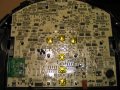
Was hoping someone could look at this schema and give me some suggestions on where to look. I can get the circuit to charge by jumping the Q18 drain and source Terminals. The PCB has two P-channel mosfets that appear to my, nearly blind eyes in this respect, to have two mosfets to accomplish the same task-battery charge. Also wondering what Mosfet Gates Drivers look like. If anyone has a minute to look at the circuits and give me an educated /experienced opinion on this I would certainly appreciate it.
Attachments
-
82.2 KB Views: 97

 Will probe this to gather data in hopes that you can tell me what particular version I am needing. Here is what I have determined so far-not much:


