 Facebook
 Google
 GitHub
 Linkedin
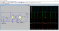
CD4013 on/off with momentary switch
- Thread starter hrs
- Start date

| Thread starter | Similar threads | Forum | Replies | Date |
|---|---|---|---|---|
|
|
Help with CD4013 for latch, then DG413 for 3PDT audio switch | Digital Design | 4 | |
|
|
CD4013 circuit flips but doesn't flop | Digital Design | 86 | |
| 4 | cd4013 flip flop outputs always on | Digital Design | 17 | |
|
|
CD4013 flip-flop | Digital Design | 12 | |
|
|
LTSpice and CD4013 | Digital Design | 12 |


