Facebook
 Google
 GitHub
 Linkedin
Hi,
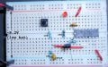
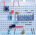
I'm trying to make an on/off button using a momentary switch and a CD4013, based on the attached diagram 4013_sch.gif taken from this site. Operation is unreliable as it will only change state some of the time. I was wondering if the debounce circuit is correct. If the switch bounces, C1 will get disconnected from CP and CP will get pulled to ground quickly through R1.
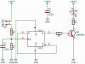
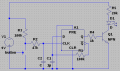
Therefore I tried another debounce circuit per second attachement, modified.png. After making the time constant R1*C1 much bigger than R2*C2 the circuit became somewhat more reliable but maybe that's just the luck of the draw. What is the purpose of the capacitor from data to ground anyway? I thought it might have something to do with flipflop racing but then I read somewhere that master-slave devices should not exhibit racing.
Would there be any benefit to putting a comparator between the debounce circuit and the clock input? Perhaps the edges are not fast enough?
I'm trying to make an on/off button using a momentary switch and a CD4013, based on the attached diagram 4013_sch.gif taken from this site. Operation is unreliable as it will only change state some of the time. I was wondering if the debounce circuit is correct. If the switch bounces, C1 will get disconnected from CP and CP will get pulled to ground quickly through R1.
Therefore I tried another debounce circuit per second attachement, modified.png. After making the time constant R1*C1 much bigger than R2*C2 the circuit became somewhat more reliable but maybe that's just the luck of the draw. What is the purpose of the capacitor from data to ground anyway? I thought it might have something to do with flipflop racing but then I read somewhere that master-slave devices should not exhibit racing.
Would there be any benefit to putting a comparator between the debounce circuit and the clock input? Perhaps the edges are not fast enough?
Attachments
-
 5.4 KB Views: 183
 -
 12.6 KB Views: 186