Cascade transistor and output resistance

Thread Starter

mondo90

Joined May 16, 2025
122
Hi,
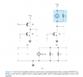
I am trying to understand how the output resistance of below very simple amplifier was calculated:
1751660917834.png

We have a cascade of two transistors Q2, Q1. The first one is a current source so we can assume no matter what the input signal is its drain current will be I. Next, we have transistor Q1 in CS configuration. If it is ON the output current is 0, inversely, when OFF output gets a total current of I. Now, what I don't get is why do we say the output resistance of Q1 is a sum of r_o1 and r_o2 in parallel as show in figure 7.3 (c)? First, output is taken across Q1 while r_o2 is between Vdd and drain of Q1 but on figure (c) it magically became connected across Q1. Second, when Q1 is OFF the current flows only through r_o2 and hence r_o1 should be infinite.
 

WBahn

Joined Mar 31, 2012
32,801
You are making two huge errors in your reasoning.

First, you are assuming that Q2 forms an ideal current source by saying that "no matter what the input signal is its drain current will be I."

In point of fact, the ability of the circuit to act as a well-behaved amplifier is reliant on the transistors NOT being ideal current sources.

Q2 is an active load and the reason that it can serve that purpose is that, as Q1 tries to change the current through it, Q2 is forced to change to a different value of current as well -- it can't stay the same. The amount of change in voltage across Q2 that corresponds to a change in the current through it is modeled by it's output resistance.

The second, and much bigger, error that you are making is trying to treat Q1 as a digital switch that is either ON or OFF. It is neither. This is an analog amplifier which biases the transistor into its intermediate region of operation in which it is always conducting and the input signal simply makes it conduct a little bit more or a little bit less. If it ever turns "on" or "off" completely, the entire point of it being an amplifier is defeated.

Finally, it's important to remember that large-signal and small-signal analysis is just a systematic way of applying the principle of superposition to the analysis of a circuit by breaking the response into two parts -- the quiescent (steady-state) response and the change in that response due to a change in the input signal, as approximated as a linear deviation from the quiescent operating point.

To understand the "magic" changes in the connections, you need to go back and relearn how you analyze circuits using superposition. You have a DC source connected between the source of Q2 and the source of Q1. That source is turned on when performing the bias portion of the analysis. This requires that it be turned off (set to zero) for all other analyses of the superposed response components. What does a voltage source that is set to zero output look like?
 

Thread Starter

mondo90

Joined May 16, 2025
122
Thank you for catching my wrong assumptions.

Q2 is an active load and the reason that it can serve that purpose is that, as Q1 tries to change the current through it, Q2 is forced to change to a different value of current as well -- it can't stay the same. The amount of change in voltage across Q2 that corresponds to a change in the current through it is modeled by it's output resistance.
Yes, having a constant current there doesn't make sense. I think the role of Q1 is just to provide some bias current.


The second, and much bigger, error that you are making is trying to treat Q1 as a digital switch that is either ON or OFF. It is neither. This is an analog amplifier which biases the transistor into its intermediate region of operation in which it is always conducting and the input signal simply makes it conduct a little bit more or a little bit less. If it ever turns "on" or "off" completely, the entire point of it being an amplifier is defeated.
No no, it's not that I think Q1 is either ON or OFF. I used these "corner" cases to show that in this situation the output resistance is not what author claims. Because if Q1 is OFF (which I think is irrational assumption here because Q2 job is to keep it in saturation) then the output resistance is just r_o2 right?

You have a DC source connected between the source of Q2 and the source of Q1
There is no DC source there, in this place we are actually taking the output v_o. The only DC sources we have are Vdd and Vg, both applied to Q2.

What does a voltage source that is set to zero output look like?
If the voltage source is 0 the circuit is shorted.

I think the reason why we take r_o1 and r_o2 in parallel as the output resistance is because in a small signal analysis (the other thread we discussed) the current can swing down to ground or up to Vdd and therefore we need to take both resistances into an account.
 

WBahn

Joined Mar 31, 2012
32,801
Yes, having a constant current there doesn't make sense. I think the role of Q1 is just to provide some bias current.
No, it provides bias current AND it acts as an active load. The latter role is the important one. If we just want to supply bias current, we could just connect the drain of Q1 to Vdd. But that would tie the output of the circuit to Vdd. If we use a passive load, we just put a resistor between Vdd and the drain of Q1. As the signal causes changes in the current in Q1, the resulting changes in voltage across the load resistor that result are the output voltage of the amplifier. The bigger we make the resistor, the bigger the changes in the output voltage for the same change in input voltage. But, the bigger resistance also pushes down the DC operating point of the output and we quickly get to the point where it forces Q1 out of saturation.

What we want is a device that has a relatively low large-signal resistance, so that the total magnitude of the voltage across it is sufficiently small at the bias current, but to have a relative high small-signal resistance, so that a small change in that current results in a relatively large change in the voltage across it.

No no, it's not that I think Q1 is either ON or OFF. I used these "corner" cases to show that in this situation the output resistance is not what author claims. Because if Q1 is OFF (which I think is irrational assumption here because Q2 job is to keep it in saturation) then the output resistance is just r_o2 right?
Again, you are confusing large signal operation with small-signal behavior.

The small-signal output resistance is the ratio of a relatively small change in the output voltage to the corresponding relatively small change in the output current. These changes have to be small enough so that the behavior is reasonably-well approximated as linear about the large-signal operating point.

It is completely unreasonable to expect that ratio to the be same at corner cases that require that the circuit deviation from the operating point is so large that the large-signal behavior transitions into a completely different mode of operation.

There is no DC source there, in this place we are actually taking the output v_o. The only DC sources we have are Vdd and Vg, both applied to Q2.
And what is the DC source known as Vdd connected to? Remember, a source has to be connected to TWO nodes in the circuit. Which two nodes in the circuit must the Vdd source be connected to in order for it to establish a voltage of Vdd between the source of Q1 and the source of Q2?

If the voltage source is 0 the circuit is shorted.
By "circuit", I hope you mean that the two nodes connected to the terminals of the voltage source are shorted.

If so, and if Vdd is shorted, what happens to the sources of Q1 and Q2?

I think the reason why we take r_o1 and r_o2 in parallel as the output resistance is because in a small signal analysis (the other thread we discussed) the current can swing down to ground or up to Vdd and therefore we need to take both resistances into an account.
That's very specious reasoning -- so much so that it's hard to comment on it.

The two resistances are in parallel because, when doing superposition with Vdd shorted, the two resistances are in parallel.

Draw the circuit with everything included, including the power and signal supplies. Then apply superposition.
 
Last edited:

LvW

Joined Jun 13, 2013
2,026
I think to find the mentioned output resistance we do not need any small signal equivalent diagram nor any other (on/off) considerations.
We only have to "look" into the output node (that means: to connect a test voltage source in our minds) and ask:
Is there only one path (or more?) for the current caused by the test voltage?
In the diagram under question I see TWO current pathes (the test current is split into two currents).
Hence, we have a parallel combination of two internal resistances.
Because we are looking into the drain node of both transistors the corresponding small-signal resistances are are ro1 and ro2.
Thats all.
 

Thread Starter

mondo90

Joined May 16, 2025
122
What we want is a device that has a relatively low large-signal resistance, so that the total magnitude of the voltage across it is sufficiently small at the bias current, but to have a relative high small-signal resistance, so that a small change in that current results in a relatively large change in the voltage across it.
Thanks, I see the intention here and it's advantages over passive components. Also, as you said this is an amplifier circuit so for this very reason the current from Q2 must change depending on the input signal but here is why I got confused - in the book Q2 is called a current source, now, what is the #1 trait of a good current source - the ability to provide an output current of a given magnitude irrespectively of the load.

Again, you are confusing large signal operation with small-signal behavior.
Right, I keep forgetting about it, I am sorry.

Which two nodes in the circuit must the Vdd source be connected to in order for it to establish a voltage of Vdd between the source of Q1 and the source of Q2?
Well, just as appears on the figure, positive terminal ad the source of Q2 and negative negative(ground) at the source of Q1. This way we have a Vdd voltage across these two transistors.

If so, and if Vdd is shorted, what happens to the sources of Q1 and Q2?
In this case, we really have the situation depicted in figure (c) - I see it now! Two resistors in parallel. However I am still a little bit blocked as to why we can short Vdd with the ground. Yes I know that this is the DC/constant source which doesn't change during small signal analysis. However, this way indicates that the current can flow upwards(from Q1 to Q2). This is similar issue that we discussed in the other thread. So, if input signal goes down the current through Q1 lowers and this is as if it would flow in the opposite direction right?


Is there only one path (or more?) for the current caused by the test voltage?
yes that is exactly how I started with my ON/OFF example (which is wrong because violated the operating point assumption). Nevertheless, I concluded current can only go downwards because v_o < Vdd always. And this is the essence of my confusion here as it suggests current goes from lower potential to a higher at times. This seems to be an useful way of describing things in so called "small-signal" analysis.
 

WBahn

Joined Mar 31, 2012
32,801
You are making progress, but still seem to get drawn into the trap of confusing large-signal and small-signal behavior.

When you say v_o < Vdd, this is the case for the TOTAL output voltage. But the total output voltage is composed of two parts, the large-signal and the small-signal.

Let's adopt the usual naming convention for these signals, which distinguish the different parts according to whether uppercase or lowercase is used.

\(
v_{OUT}(t) \; = \; V_{OUT} \; + \; v_{out}(t)
\)

On the left is the total signal at the output, which is written using lowercase for the variable name but uppercase for the subscript.

The first term on the right is the DC, or quiescent, or large-signal, or bias component, which is a constant. It is written using uppercase for both the variable and the subscript.

The second term on the right is the AC, or small-signal, component. It is written using lowercase for both the variable and the subscript.

It is true that, in this circuit, the TOTAL output voltage is always at least 0 V but no more than Vdd, but this does NOT say the small-signal voltage can't be negative.

\(
0 \; \le \; v_{OUT}(t) \; \le \; V_{DD} \\
0 \; \le \; V_{OUT} \; + \; v_{out}(t) \; \le \; V_{DD} \\
-V_{OUT} \; \le \; \; v_{out}(t) \; \le \; V_{DD} \; - \; V_{OUT}
\)

Remember, if v_out is negative, it does NOT mean that current is flowing from a lower potential to a higher potential. It merely means that the TOTAL output voltage is LESS than the QUIESCENT output voltage.

Let's say that V_DD = 10 V and V_OUT = 6 V.

If v_out happens to be -2 V, the total output voltage is 6 V + (-2 V) which is 4 V. The physical circuit only knows about the total signals -- it has no awareness of how we have chosen to mathematically break a signal into component pieces.

You really need to take a step back and spend some time with basic circuit analysis, focusing on superposition. I'm not talking about just memorizing what the steps are and how to apply them, I'm talking about making sure that you understand where those steps come from and why they are valid.
 

LvW

Joined Jun 13, 2013
2,026
....................
Nevertheless, I concluded current can only go downwards because v_o < Vdd always. And this is the essence of my confusion here as it suggests current goes from lower potential to a higher at times. This seems to be an useful way of describing things in so called "small-signal" analysis.
Your conclusion ("current can only go downwards") is false.
The wanted quantity (ro) is a small-signal parameter - hence, we have to do with small signals equations only.
You must not mix DC voltages (Vdd) with small voltage changes (signal voltages).
For such signal voltages the DC source is identical to common ground and, therefore, the signal test current goes both ways.
(This is the fundamental basis and the most important property of the small-signal equivalent circuit diagram).
 
Last edited:

Thread Starter

mondo90

Joined May 16, 2025
122
WBahn, thanks for your response, I am progressing indeed but still some things are hard to accept for me:

Remember, if v_out is negative, it does NOT mean that current is flowing from a lower potential to a higher potential. It merely means that the TOTAL output voltage is LESS than the QUIESCENT output voltage.
If I understand correctly this is because, let's say at this instant V_o = V_O + v_o where LHS term is output voltage (DC + signal), V_O is the DC bias value, v_o signal, then if v_o changes, so that the output goes above the bias output voltage V_O, then we temporarily have a situation that V_o > V_O and hence current flows from Q1 towards Q2 - this is the confusing situation which looks like if the current flows from lower potential (ground) to a higher (Vdd), am I right?

When you say "Remember, if v_out is negative" I assume you mean negative in regards to the DC bias, not to ground.

The second, and much bigger, error that you are making is trying to treat Q1 as a digital switch that is either ON or OFF... If it ever turns "on" or "off" completely, the entire point of it being an amplifier is defeated.
Getting back to this point again, the gate of Q1 is a plain signal v_i, no DC bias, no nothing. This means, if the gate to source voltage V_gs is below certain threshold then Q1 is completely OFF, so I was right with my ON/OFF interpretation right? The only bias I see is on the gate of Q2.

You really need to take a step back and spend some time with basic circuit analysis, focusing on superposition.
Thank you for this suggestion. I think I understand a superposition well, I worked through examples where when we turn off independent sources one by one calculate their contributions to a particular signal separately and then add them all together. I am not sure if this has a direct application here. I am getting confused by things like this:
1751910386668.png


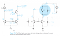
For the circuit on the left we are asked to calculate the output resistance. To that end author turns off the I_ref (this is clear), and applies test voltage to the output so later, knowing current at this point he can calculate the resistance from R = V/I formula (also clear). However, observe what currents does the test voltage produce - current i_x creates i_2 current flowing out of the base of Q2, this is not how a BJT transistor works right? Second, this i_2 current is said to be aprox. equal to i_1 (due to current mirroring) but that would mean the collector current is almost entirely a base current, making beta of Q3 equal around 1. Not very realistic. not to mention the collector current goes in the opposite direction of emitter current.

Additional points:
1. author says "we have “pulled out” r_o of each transistor and shown it separately" but if that is the output resistance shouldn't it be in series with the transistor?
2. author says "current i_2 flows into the base of Q3 and gives rise to a collector current B_3*i_2 and then in following calculations he also makes an assumption that B_3 (beta of Q3) is much bigger than 2 - both of these statements contradict what I see on the schematic.
 

LvW

Joined Jun 13, 2013
2,026
1. author says "we have “pulled out” r_o of each transistor and shown it separately" but if that is the output resistance shouldn't it be in series with the transistor?
For a non-ideal voltage source, the internal resistor is in series with the source.
For a non-ideal current source, the internal resistor is in parallel with the source.
 

Thread Starter

mondo90

Joined May 16, 2025
122
For a non-ideal voltage source, the internal resistor is in series with the source.
For a non-ideal current source, the internal resistor is in parallel with the source.
Ok, so in essence Norton and Thevenin source transformation
 

WBahn

Joined Mar 31, 2012
32,801
If I understand correctly this is because, let's say at this instant V_o = V_O + v_o where LHS term is output voltage (DC + signal), V_O is the DC bias value, v_o signal, then if v_o changes, so that the output goes above the bias output voltage V_O, then we temporarily have a situation that V_o > V_O and hence current flows from Q1 towards Q2 - this is the confusing situation which looks like if the current flows from lower potential (ground) to a higher (Vdd), am I right?
No, you are not right, and your reasoning demonstrates that, regardless of what you may think, you do not understand what superposition is. Whether you can successfully apply the steps of an algorithm says little about whether you understand how and why that algorithm works and is valid. This is not at all uncommon. Most people can operate an automatic transmission. Very few people know how and why it works, even in principle, let alone in reality. But there are things that we really should know and understand what is going on under the hood and, for an electrical engineer, understanding the underlying concepts of superposition and how they underpin small-signal analysis is pretty high on that list.

Let's consider a very simplified example to illustrate superposition. At each step, I'm going to ask you to consider whether you agree with a certain claim. This is not meant to be demeaning in any way. It is merely a request that you pause at those points and consider whether you truly understand and agree with the claim being made. If you don't, then that is a point where we need to stop and delve deeper to get you to that point (or, possibly, that I've blundered and fat-fingered an equation, or worse, but that is something that is even more critical that we identify and resolve).

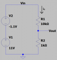
1751913809696.png


Would you agree that the current, Io, in R1 and R2, and that the voltage at the output, Vout, are given by the following expressions?

\(
i_O \; = \; \frac{V_1 \; + \; V_2}{R_1 \; + \; R2}
\)

\(
v_{out} \; = \; i_o \cdot R_2 \; = \; \left(V_1 \; + \; V_2\right) \cdot \frac{R_2}{R_1 \; + \; R2}
\)

For the values shown, would you agree that these yield the following values?

\(
i_O \; = \; \frac{11\;V \; - \; 1.1\;V}{10\;k\Omega \; + \; 1\;k\Omega} \; = \; 0.9\;mA
\)

\(
v_{out} \; = \; 0.9\;mA \cdot 1\;k\Omega \; = \; \left(11\;V \; - \; 1.1\;V \right) \cdot \frac{1\;k\Omega}{10\;k\Omega \; + \; 1\;k\Omega} \; = \; 0.9\; V
\)

Would you agree that, if what we want to know is this current and this voltage in this circuit, that the analysis is done and we have our answers?

Would you agree that current is flowing downward in both resistors?

Would you agree that current is NOT flowing from a lower potential to a higher potential at any point in this circuit?

So now let's do nothing more than reorganize these equations.

Would you agree that I can reorganize these equations to write them as follows?

\(
\begin{align}
i_O \; &= \; \frac{V_1 \; + \; V_2}{R_1 \; + \; R2} \\
&= \; \frac{V_1}{R_1 \; + \; R2} \; + \; \frac{V_2}{R_1 \; + \; R2} \\
\end{align}
\)

\(
\begin{align}
v_{out} \; &= \; \left(V_1 \; + \; V_2 \right) \cdot \frac{1\;k\Omega}{10\;k\Omega \; + \; 1\;k\Omega} \\
&= \; V_1 \cdot \frac{R_2}{R_1 \; + \; R2} \; + \; V_2 \cdot \frac{R_2}{R_1 \; + \; R2}
\end{align}
\)

Would you agree that I am free to define the following new variables?

\(
I_O \; = \; \frac{V_1}{R_1 \; + \; R2} \\
\\
i_o \; = \; \frac{V_2}{R_1 \; + \; R2} \\
\\
V_{OUT} \; = \; V_1 \cdot \frac{R_2}{R_1 \; + \; R2} \; \\
\\
v_{out} \; = \; V_2 \cdot \frac{R_2}{R_1 \; + \; R2}
\)

If I evaluate these new variables, do you agree that I get the following results?

\(
I_O \; = \; \frac{V_1}{R_1 \; + \; R2} \; = \; \frac{11\;V}{10\;k\Omega \; + \; 1\;k\Omega} \; = \; 1.0\;mA\\
\\
i_o \; = \; \frac{V_2}{R_1 \; + \; R2} \; = \; \frac{-1.1\;V}{10\;k\Omega \; + \; 1\;k\Omega} \; = \; -0.1\;mA\\
\\
V_{OUT} \; = \; V_1 \cdot \frac{R_2}{R_1 \; + \; R2} \; \; = \; 11\;V \cdot \frac{1\;k\Omega}{10;k\Omega \; + \; 1\;k\Omega} \; = \; 1.0\;V\\
\\
v_{out} \; = \; V_2 \cdot \frac{R_2}{R_1 \; + \; R2} \; = \; -1.1\;V \cdot \frac{1\;k\Omega}{10;k\Omega \; + \; 1\;k\Omega} \; = \; -0.1\;V
\)

Would you agree that I can use these new variables to express the previous equations as the following?

\(
i_O \; = \; I_O \; + \; i_o \\
\\
v_{out} \; = \; V_{OUT} \; + \; v_{out}
\)

Would you agree that these evaluate to the following?

\(
i_O \; = \; I_O \; + \; i_o \; = \; 1.0\;mA \; - \; 0.1\;mA \; = \; 0.9\;mA \\
\\
v_{out} \; = \; V_{OUT} \; + \; v_{out} \; = \; 1.0\;V \; - \; 0.1\;V \; = \; 0.9\;V
\)

Would you still agree that current is flowing downward in both resistors?

Would you still agree that current is NOT flowing from a lower potential to a higher potential at any point in this circuit?

Do you agree that this is the case even though both i_0 and v_out are negative?

The key is that NONE of the new variables that I introduced are REAL currents or voltages. They are "virtual" currents and voltages that exist ONLY as mathematical components in the equations that yield the "actual" or "physical" currents and voltages.

When we split the real equations into sets of virtual components, we can't mix and match. When applying superposition, we are essentially assigning each independent source to either the large-signal virtual circuit or the small-signal virtual circuit. We must assign it to exactly one -- we cannot ignore it altogether, and we cannot assign it to both. Each virtual circuit is then its own self-contained universe. We cannot mix and match them. In your transistor circuit. Vdd is part of the large-signal virtual circuit, as is V_OUT. But v_i and v_out are part of the small-signal virtual circuit. We CANNOT compare v_out to VOUT. They simply are not comparable quantities.

Getting back to this point again, the gate of Q1 is a plain signal v_i, no DC bias, no nothing. This means, if the gate to source voltage V_gs is below certain threshold then Q1 is completely OFF, so I was right with my ON/OFF interpretation right? The only bias I see is on the gate of Q2.
This is a point that I noticed immediately and have chosen to sit on my hands about up until now.

The author is being a bit sloppy here. They may well have established a convention previously in the text to explain the shortcut they are taking here (which, being fair, is a pretty common one).

They are leaving out the bias voltage generator for the gate of Q1 and drawing the circuit as though v_i (which, per the naming convention, is just the small-signal component of the total input signal) were applied directly to it. In order for the circuit to operate as an amplifier, the gate of Q1 must be DC biased to a value that results in the same current flowing in Q1 as is flowing in Q2 when the voltage at the drains are at about the midpoint of the supply voltage. The details of how this is done are not important to analyzing the small-signal response, so the author is being a bit sloppy and ignoring it altogether. It would have been better if they had written the voltage on that gate as the sum of a bias voltage and signal voltage, though that would probably have resulted in other students getting confused.

EDIT: Fix typos
 
Last edited:

Thread Starter

mondo90

Joined May 16, 2025
122
Thanks for the great example, let's zoom in where the misunderstanding is:

View attachment 352318


Would you agree that the current, Io, in R1 and R2, and that the voltage at the output, Vout, are given by the following expressions?

\(
i_O \; = \; \frac{V_1 \; + \; V_2}{R_1 \; + \; R2}
\)

\(
v_{out} \; = \; i_o \cdot R_2 \; = \; \left(V_1 \; + \; V_2\right) \cdot \frac{R_2}{R_1 \; + \; R2}
\)
Yes, this is simple Ohm's law / Voltage divider formula derived.
For the values shown, would you agree that these yield the following values?

\(
i_O \; = \; \frac{11\;V \; - \; 1.1\;V}{10\;k\Omega \; + \; 1\;k\Omega} \; = \; 0.9\;mA
\)

\(
v_{out} \; = \; 0.9\;mA \cdot 1\;k\Omega \; = \; \left(11\;V \; - \; 1.1\;V \right) \cdot \frac{1\;k\Omega}{10\;k\Omega \; + \; 1\;k\Omega} \; = \; 0.9\; V
\)
Yes.
Would you agree that, if what we want to know is this current and this voltage in this circuit, that the analysis is done and we have our answers?
Yes.
Would you agree that current is flowing downward in both resistors?
Yes, because despite the fact V2 is negative, the combined voltage is still positive. If V2 changed from -1.1V to say -11.1V the current direction would have changed. But I don't think it is important here.
Would you agree that current is NOT flowing from a lower potential to a higher potential at any point in this circuit?
Yes.
Would you agree that I can reorganize these equations to write them as follows?


\(
\begin{align}
i_O \; &= \; \frac{V_1 \; + \; V_2}{R_1 \; + \; R2} \\
&= \; \frac{V_1}{R_1 \; + \; R2} \; + \; \frac{V_2}{R_1 \; + \; R2} \\
\end{align}
\)

\(
\begin{align}
v_{out} \; &= \; \left(V_1 \; + \; V_2 \right) \cdot \frac{1\;k\Omega}{10\;k\Omega \; + \; 1\;k\Omega} \\
&= \; V_1 \cdot \frac{R_2}{R_1 \; + \; R2} \; + \; V_2 \cdot \frac{R_2}{R_1 \; + \; R2}
\end{align}
\)
Yes, this is in essence the superposition.
Would you agree that I am free to define the following new variables?

\(
I_O \; = \; \frac{V_1}{R_1 \; + \; R2} \\
\\
i_o \; = \; \frac{V_2}{R_1 \; + \; R2} \\
\\
V_{OUT} \; = \; V_1 \cdot \frac{R_2}{R_1 \; + \; R2} \; \\
\\
v_{out} \; = \; V_2 \cdot \frac{R_2}{R_1 \; + \; R2}
\)

If I evaluate these new variables, do you agree that I get the following results?

\(
I_O \; = \; \frac{V_1}{R_1 \; + \; R2} \; = \; \frac{11\;V}{10\;k\Omega \; + \; 1\;k\Omega} \; = \; 1.0\;mA\\
\\
i_o \; = \; \frac{V_2}{R_1 \; + \; R2} \; = \; \frac{-1.1\;V}{10\;k\Omega \; + \; 1\;k\Omega} \; = \; -0.1\;mA\\
\\
V_{OUT} \; = \; V_1 \cdot \frac{R_2}{R_1 \; + \; R2} \; \; = \; 11\;V \cdot \frac{1\;k\Omega}{10;k\Omega \; + \; 1\;k\Omega} \; = \; 1.0\;V\\
\\
v_{out} \; = \; V_2 \cdot \frac{R_2}{R_1 \; + \; R2} \; = \; -1.1\;V \cdot \frac{1\;k\Omega}{10;k\Omega \; + \; 1\;k\Omega} \; = \; -0.1\;V
\)
Yes.
Would you agree that I can use these new variables to express the previous equations as the following?

\(
i_O \; = \; I_O \; + \; i_o \\
\\
v_{out} \; = \; V_{OUT} \; + \; v_{out}
\)
Yes.
Would you agree that these evaluate to the following?

\(
i_O \; = \; I_O \; + \; i_o \; = \; 1.0\;mA \; - \; 0.1\;mA \; = \; 0.9\;mA \\
\\
v_{out} \; = \; V_{OUT} \; + \; v_{out} \; = \; 1.0\;V \; - \; 0.1\;V \; = \; 0.9\;V
\)
Yes.
Would you still agree that current is flowing downward in both resistors?
Yes.
Would you still agree that current is NOT flowing from a lower potential to a higher potential at any point in this circuit?
Yes.
Do you agree that this is the case even though both i_0 and v_out are negative?
Yes.
The key is that NONE of the new variables that I introduced are REAL currents or voltages. They are "virtual" currents and voltages that exist ONLY as mathematical components in the equations that yield the "actual" or "physical" currents and voltages.
Yes, I understand it. So to wrap up, all above analysis seems to be clear and for the circuit from my first post I agree that there will be no current flowing upwards towards Q2. If the output goes down it is because Q1 conducts more and sinks outputs current.
But then we have this, from the other, similar thread we discussed:
1751943414997.png
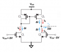
While I see the doubled current mathematically: increased by delta from Q4 + changed by -delta in Q2, which we understand as flowing upwards. Then using KCL, we have 2 deltas at the output - all of that makes sense beside the arrow blue arrow pointing up on the above schematic. I believe this is not depicting the actual situation taking place in the circuit but rather helps to visualize the increased output current which in fact is all produced by Q4 mirror.


This is a point that I noticed immediately and have chosen to sit on my hands about up until now.

The author is being a bit sloppy here. They may well have established a convention previously in the text to explain the shortcut they are taking here (which, being fair, is a pretty common one).
Ok, but his intention was to have it all biased at certain level so we should only focus on small signal analysis.
 

WBahn

Joined Mar 31, 2012
32,801
But then we have this, from the other, similar thread we discussed:
View attachment 352326
While I see the doubled current mathematically: increased by delta from Q4 + changed by -delta in Q2, which we understand as flowing upwards. Then using KCL, we have 2 deltas at the output - all of that makes sense beside the arrow blue arrow pointing up on the above schematic. I believe this is not depicting the actual situation taking place in the circuit but rather helps to visualize the increased output current which in fact is all produced by Q4 mirror.
Again, neither the blue or the red arrows depict actual currents -- well, the red ones match the actual currents in the very specific situation in which the blue ones are identically zero. This is the case when the small signal portion of the input, ΔV, happens to be zero. But the blue arrows can never be the actual currents because V_CM can't be zero and still have the circuit operating at a point where we can linearize it about that point in any meaningful way.

This is no different than when you do mesh current analysis and have two mesh currents, flowing in opposite directions, through a branch. In general, neither mesh current is the actual current. The actual current is their difference.

Here we point the blue current upward as a convenience. We could just as easily point it downward, but then we would have to have labeled it as -ΔI. In either case, the total current flowing downward into Q2 is Io-ΔI. But we like to avoid minus signs as much as possible because we humans are much more likely to mess something up the more we are forced to deal with them.

Ok, but his intention was to have it all biased at certain level so we should only focus on small signal analysis.
Correct.

This has to be the case, because superposition is only valid for linear systems. But transistors are strongly non-linear devices. So, in order for us to use all of our powerful analysis and design techniques that only apply to linear systems, we must force our non-linear system to operate over a sufficiently small range such that we can approximate it as being linear about some operating point. The large-signal portion captures the non-linear behavior enough to get the operating point. The small-signal portion describes the linear approximation of how the circuit behaves in the vicinity of the operating point.
 

Thread Starter

mondo90

Joined May 16, 2025
122
well, the red ones match the actual currents in the very specific situation in which the blue ones are identically zero.
Only in this situation? I though you marked the DC current by the red arrows and while theirs magnitude may change, theirs direction will always be like on the diagram?
But the blue arrows can never be the actual currents because V_CM can't be zero and still have the circuit operating at a point where we can linearize it about that point in any meaningful way.
Exactly, that was the source of my confusion from the very beginning. It seems to be a nice method to visualize the increased output current but does not depict what's going on in the real world. Now, what is going on in the real world so that the output current is doubled? First, I believe the output current is dependent on the load resistance - for instance, if we short the output terminal, it will sink all the current that Q2 tries to sink regardless of Q2s gate input signal, right? Second, In the case where Q1s gate is + delta signal while Q2s gate is -delta signal, Q2 sinks less current therefore output load can take 2x delta current but in fact all that current is produced by Q4 mirror. Am I right?

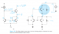
Also, can you help me go through this:
1752012576127.png

First why can we treat Q3 as a supernode? A supernode by definition is formed by a voltage source connected between two non reference nodes and anything in parallel with it. Here however, when author calculates the output resistance by connecting the test voltage Vx to the Q3s collector, that node is a refference node - we know it's voltage right?
Even assuming it is ok, how can he conclude that:
1. Collector current is Beta_3*i_2, emitter current is i_1 and they are not equal or at least approximately equal? In BJTs, the collector and emitter currents should be almost identical.
2. Next, how can he say that i_2 and i_1 are identical - that would mean all of the emitter current comes from the base - exact opposite of what it is in the reality.
3. Maybe not that important but how can a a direction of base current be flowing out of the transistor and yet we assume it all "works" fine.

Thanks.
 

WBahn

Joined Mar 31, 2012
32,801
3. Maybe not that important but how can a a direction of base current be flowing out of the transistor and yet we assume it all "works" fine.

Thanks.
Once again, you insist on treating a small-signal variable as if it were the only thing in the actual circuit. A small-signal flowing out of the base of an NPN transistor means nothing more than that the total (actual) current going into the base is LESS than the quiescent current.

I'll try to address your other questions later when I have some more time.

One thing that this author seems to do which, I think, adds needlessly to the confusion is to draw the small-signal quantities on the schematic with the transistor symbols. While doing this is a common shortcut people use once they are comfortable with thinking of the small-signal situation in isolation, I think it can confuse people, like you, that are struggling to get the concept down. I believe the better way is to first develop the small signal models by deriving them directly from the constitutive equations for the non-liner devices (which, hopefully, the author did at some earlier point in the work) and then make a clean break between large-signal and small-signal circuits. Use the transistor symbols in the full schematic and determine the DC operating point. Then draw a new schematic that replaces the transistors with their small-signal equivalents and zero out the DC supplies to yield the circuit that the small-signal sees.
 

LvW

Joined Jun 13, 2013
2,026
One thing that this author seems to do which, I think, adds needlessly to the confusion is to draw the small-signal quantities on the schematic with the transistor symbols.
................
................
Then draw a new schematic that replaces the transistors with their small-signal equivalents and zero out the DC supplies to yield the circuit that the small-signal sees.
Yes, I fully agree with these considerations.
Furthermore, I am even of the opinion that the small-signal equivalent circuit diagrams are actually superfluous and sometimes even complicate the calculation and/or lead to errors.
These equivalent circuit diagrams are nothing more than a visualization of the classical equations for describing the behaviour of the transistor as an amplifier.
If you know these equations, you don't need any equivalent circuit diagram.
In most cases, there are only two smal-signal equations which really matter:
ic=gm*vbe and Ib=ic/beta.
 

WBahn

Joined Mar 31, 2012
32,801
Yes, I fully agree with these considerations.
Furthermore, I am even of the opinion that the small-signal equivalent circuit diagrams are actually superfluous and sometimes even complicate the calculation and/or lead to errors.
I don't agree, especially for someone just learning how to analyze and design these circuits.

These equivalent circuit diagrams are nothing more than a visualization of the classical equations for describing the behaviour of the transistor as an amplifier.
But that's all any circuit diagram is -- a way to visualize the mathematical relationships of the circuit. But that doesn't mean that by knowing the constitutive equations for resistors, capacitors, and inductors that I can easily dispense with the circuit diagrams for an RLC filter.

If you know these equations, you don't need any equivalent circuit diagram.
In most cases, there are only two smal-signal equations which really matter:
ic=gm*vbe and Ib=ic/beta.
That might be sufficient for determining the simplest approximation of the amplifier behavior in one of the classic configurations, but it's not going to get you very far when you start dealing with the impact of internal parasitics, particularly when their interactions with the external components, including with the parasitics in other transistors, start dominating the behavior.
 

LvW

Joined Jun 13, 2013
2,026
LvW said:
Furthermore, I am even of the opinion that the small-signal equivalent circuit diagrams are actually superfluous and sometimes even complicate the calculation and/or lead to errors.
I don't agree, especially for someone just learning how to analyze and design these circuits.
Let me tell you that my opinion is the result of experience with some students - especially beginners.

The classical rules for circuit calculation (Kirchhoff's laws) are often applied to these equivalent circuit diagrams in a very formalistic way, which certainly leads to the correct result (if no mistakes are made).
However, a good understanding of how the transistor really works is not retrieved.

More than that - unfortunately, there exist two equivalent circuit diagrams which do not correctly reflect the physical functioning of the transistor:
(1) Although the BJT is a voltage-controlled element (current source ic=gm*vbe), it is often shown as current-controlled (ic=beta*ib).
(2) Even more confusing is the so-called "T-equivalent circuit" with a quantity re, which is referred to as "intrinsic emitter resistance".
This is nothing else than the inverse transconductance (re=1/gm), which of course does not belong to the emitter and is also not an "internal resistance".

If applied correctly, the results will be not wrong - however, both equivalent circuits mislead many beginners into a completely false understanding of the physically correct operation of the BJT.
(I can`t even guess how many people - not only beginners - think that the BJT is a current-controlled element).

As an example, lets assume that I am a beginner and want to find the gain of a designed simple common emitter stage (with a capacitor Ce across the emitter resistor). All resistor values are known. I am using a small-signal diagram with the current source ic=beta*ib.
Using Ohms law and the definition of gain I arrive at:
v_out=-ic*Rc=-beta*ib*Rc
ib=v_in/rbe
v_out/v_in=G=-beta*Rc/rbe.

And now? Who gives me reliable values for beta and rbe?
(I am a beginner and do not know that the ratio beta/rbe is a quantity that is known from the DC operating point)

Do you now understand my reservations against the use of such diagrams without a good understanding of the BJT physics?
 
Last edited:

WBahn

Joined Mar 31, 2012
32,801
The classical rules for circuit calculation (Kirchhoff's laws) are often applied to these equivalent circuit diagrams in a very formalistic way, which certainly leads to the correct result (if no mistakes are made).
However, a good understanding of how the transistor really works is not retrieved.
This strikes me as largely apples and oranges. Let's use a basic inductor as an example. Being able to work with the equation that govern it, namely V=L·di/dt, doesn't imply any understanding of how it really works. Similarly, having a good understanding of how it works doesn't imply an ability to understand, analyze, or design circuits that use inductors. These are largely separate things that, while they work best when they complement each other, are somewhat orthogonal.

More than that - unfortunately, there exist two equivalent circuit diagrams which do not correctly reflect the physical functioning of the transistor:
(1) Although the BJT is a voltage-controlled element (current source ic=gm*vbe), it is often shown as current-controlled (ic=beta*ib).
(2) Even more confusing is the so-called "T-equivalent circuit" with a quantity re, which is referred to as "intrinsic emitter resistance".
This is nothing else than the inverse transconductance (re=1/gm), which of course does not belong to the emitter and is also not an "internal resistance".

If applied correctly, the results will be not wrong - however, both equivalent circuits mislead many beginners into a completely false understanding of the physically correct operation of the BJT.
(I can`t even guess how many people - not only beginners - think that the BJT is a current-controlled element).
Yet I'll bet even you treat it that way much of the time.

Let's say that I have a typical small-signal NPN transistor and a 12 V supply. I connect the emitter to the negative terminal, which I use as my common reference node, and the base and collector to the positive terminal via two resistors, a 1 kΩ resistor at the collector and a 220 kΩ resistor at the base. I measure the collector voltage and find it to be 3 V. What value should I change the resistor to in order to get the collector voltage to near 6 V?

Are you going to insist that the transistor cannot be treated as a current-controlled element and figure out what Vbe is and then figure out what the change in Vbe needs to be in order to result in the needed change in collector current, and then figure out what the value of the base resistor is that will result in that Vbe?

Or are you going to determine that you need the collector current to go from 9 mA to 6 mA (i.e., be 2/3 of the original amount) and, treating it as a current-controlled current source, conclude that the base resistor's current needs to be scaled by the same amount and, hence, needs the resistance to be scaled by a factor of about 3/2, making it about 330 kΩ?

As an example, lets assume that I am a beginner and want to find the gain of a designed simple common emitter stage (with a capacitor Ce across the emitter resistor). All resistor values are known. I am using a small-signal diagram with the current source ic=beta*ib.
Using Ohms law and the definition of gain I arrive at:
v_out=-ic*Rc=-beta*ib*Rc
ib=v_in/rbe
v_out/v_in=G=-beta*Rc/rbe.

And now? Who gives me reliable values for beta and rbe?
(I am a beginner and do not know that the ratio beta/rbe is a quantity that is known from the DC operating point)
I would hope that this beginner wasn't just given either the tee model or the hybrid-pi small-signal model for a BJT and, instead, was walked through the development of where they both came from starting with the Ebers-Moll model and applying the defining concepts of small-signal analysis to arrive at those equivalent circuits, and hence see the explicit tie between them and the DC operating point.

Do you now understand my reservations against the use of such diagrams without a good understanding of the BJT physics?
What I don't see is how using such diagrams implies or requires a poor understanding of the BJT physics.

The same argument could be made about the use of many standard analysis and design techniques. Indeed, this thread (an many before it) underscore the tendency to confuse mathematical constructs, such as superposition and small-signal components, with real-world voltages and currents. But that doesn't mean that we should abandon those techniques, only that we need to do a better job at teaching them -- and recognize that we need to stop taking the attitude that presenting them once, when they are first introduced, is satisfactory. The fundamentals need to be revisited and reemphasized multiple times for them to really sink in. This is something that most curricula (in most areas) fails to do.

EDIT: Fix quote tags.
 
Last edited:
Top