 Facebook
 Google
 GitHub
 Linkedin
Hello,
I am trying to get +3V/-3V square signal from Q5 of CD4024B but since I'm not able to change Vss value of the IC, I get +3V / 0V signal instead of +3V/-3V signal. Can you show me a way to arrange it?
Additional Info: In fact, my main purpose is getting the signal from Q4 of CD4060B but my lib includes CD4060Bg and it both doesn't work and has the same problem also.
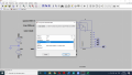
The files are attached. As you can see, if there were any pin for VDD and VSS, I would label them and use the voltage sources on the left side. Because no pins exist, I tried to edit properties but only VDD was shown. I can change it by editing or parametrizing but I need to change VSS. Need your help.
Thanks, regards...
I am trying to get +3V/-3V square signal from Q5 of CD4024B but since I'm not able to change Vss value of the IC, I get +3V / 0V signal instead of +3V/-3V signal. Can you show me a way to arrange it?
Additional Info: In fact, my main purpose is getting the signal from Q4 of CD4060B but my lib includes CD4060Bg and it both doesn't work and has the same problem also.
The files are attached. As you can see, if there were any pin for VDD and VSS, I would label them and use the voltage sources on the left side. Because no pins exist, I tried to edit properties but only VDD was shown. I can change it by editing or parametrizing but I need to change VSS. Need your help.
Thanks, regards...
Attachments
-
2 KB Views: 11
-
 422.8 KB Views: 16
 -
 26.5 KB Views: 12

") Actually I'm not used to LTspice, so I don't know how to do arrangements that you told.
Actually I'm not used to LTspice, so I don't know how to do arrangements that you told.


