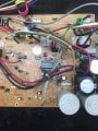
Can you help identify this IC from an air-condition outdoor unit

Status
Not open for further replies.

Kjeldgaard

Joined Apr 7, 2016
476
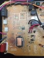
I see a few strange things in the picture in post #1:

Jumper J167 (bottom left) seems to be burned?

Is there a crack in the PCB at the bottom left, just off the C118 text?
 

Thread Starter

Yami

Joined Jan 18, 2016
354
Hey guys here is the pictures of the full board, yes the corner of the board has snapped of I'm guessing due to the impact. The fuses seems to be ok, and no visual damaged could be seen from the components.
1.jpg
21.jpg
 

Thread Starter

Yami

Joined Jan 18, 2016
354
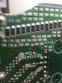
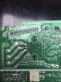
Now here is the weird thing - the jumper which snapped off doesn't actually bridge anything. It seems to be on the same pad (you know what I mean right). I have circled that in red. There was a surface mount resistor close to it which was burned out, and also the other weird thing . I checked the resistance across couple of them and it showed a dead short - I figured it could be the burnt one as all them were connected in parallel. So I removed the burnt resistor and still resistors measured as a dead short, as if the pad was bypassing them. What is this 'wizadry' o_O
5.jpg
4.jpg
 

MisterBill2

Joined Jan 23, 2018
27,998
A bunch of small resistors in parallel is the simple way to have a lower resistance at a higher power rating. and 14 one ohm resistors in parallel would be close to short circuit on most ohm meters. And I see that board has a big crack that has broken some traces. The first photo shows some heat effects to the left of the big IC device.
 

Thread Starter

Yami

Joined Jan 18, 2016
354
A bunch of small resistors in parallel is the simple way to have a lower resistance at a higher power rating. and 14 one ohm resistors in parallel would be close to short circuit on most ohm meters. And I see that board has a big crack that has broken some traces. The first photo shows some heat effects to the left of the big IC device.
I see, so could I get a way without replacing that burnt resistor? As that is not avilable here. What could possibly be the use of this resistor network?
The crack doesn't seem to cause any connection to be bad
 

Ylli

Joined Nov 13, 2015
1,092
My first thought was "why did that -one- resistor fry with all those other equal values resistors in parallel". Well, with that crack where it is, all the current may have been funneled though the one resistor (instead of being spread among the 14) and that is why it is fried.
 

ebp

Joined Feb 8, 2018
2,332
I agree that the crack forced all the current that should flow through the parallel combination of the resistors through the one that is blow, ultimately isolating the black wire in the corner of the board. The crack will probably electrically re-close easily but would be incapable of carrying more than a very small current. It needs to be properly repaired.

Was J167 just broken? It really looks to me like the free end has be melted, but it is hard to tell for sure from the photos.

===
The board is a single-sided type made using cheap materials and cheap (for high volume) methods. The substrate is phenolic-paper, which is the cheapest available. Boards like that used to be imaged for etching with offset printing techniques, but I don't know if that is usable with the finer features required for modern parts. Screen printing was also used. Phenolic laminate is horrible to drill because it gunks up the drills - and stinks! The boards are punched, instead, presumably using a single multi-pin punch with matching die to make all the holes in one whack. Note some of the holes are rectangular. In epoxy-glass laminate that would require routing and would be expensive. Some grades of phenolic need to be heated for punching, some will punch OK when cold. Mechanical strength is vastly lower than for epoxy-glass laminates. These types of boards are quite common in consumer equipment. It amazes me that it is cheaper to insert a ton of jumpers rather than use a double sided board, but it is. I assume the jumper wires are formed and cut by the insertion machinery.
 

Thread Starter

Yami

Joined Jan 18, 2016
354
I still don't understand the point of the jumper. It doesn't seem to connect to anything. It snapped off when I was cleaning it, but yes it does look like one end of it has suffered some ill effects from heat.
The whole bottom of the board is covered with some kind of clear silicone type material. I had to scrap it off at the points I had to de-solder.
 

MisterBill2

Joined Jan 23, 2018
27,998
I still don't understand the point of the jumper. It doesn't seem to connect to anything. It snapped off when I was cleaning it, but yes it does look like one end of it has suffered some ill effects from heat.
The whole bottom of the board is covered with some kind of clear silicone type material. I had to scrap it off at the points I had to de-solder.
The crack and the broken off piece removed a connection of something. So that may even be why the compressor does not run any more. Patching the crack would not be that hard, and replacing the missing piece may be important..
 

ebp

Joined Feb 8, 2018
2,332
That jumper is strange. The only possible purpose I can see for it is as some sort of test point. There are a number of strange things on the board - note there are small holes that seem to have nothing to do with anything near that jumper and some others elsewhere. I wonder if perhaps the board was revised and both the jumper and the apparently useless holes are remnants. I've never been involved in high volume consumer electronics design, so some of these things shall forever remain a mystery to me.

Those paralleled resistors probably are used for a current sensing function, in which case loss of one of the 14 would reduce the current (presumably) limit by about 7%. I doubt if that will make a big difference to operation. My guess is that it would slow the start-up of the (compressor?) a little and probably make no difference at all once it was running.

Surface mount resistors of that size are not terribly difficult to hand solder with an iron and won't be damaged if care is used (unlike ceramic capacitors, where soldering with an iron is always dubious). However, the board certainly looks like it has been wave soldered, which would mean all of the components are "glued" in place before soldering. This can make removal difficult.
 

MisterBill2

Joined Jan 23, 2018
27,998
In the second image in the pictures of post #33 it looks like smoke evidence on the base of the red and orange wires, which says that some part made that smoke while failing..
AND, I see two corners broken off of the board, and along with seeing the cracks that are not repaired and the missing trace at the missing corner, I am thinking that there are probably other broken traces on the board, resulting in additional open circuits. So that could be the reason why some portion is not working. A control circuit is not like a test, where 85% is OK. And I saw at least one additional crack on a top view. Besides that I see where Q1 , a transistor, has been unsoldered and removed, and white tape next to that area hiding something ugly. So there is far more than is being presented here. It is quite possible that the board should be replaced if you can't see the problems to repair them.
 
Status
Not open for further replies.
Top