Facebook
 Google
 GitHub
 Linkedin
Sedra & Smith Microelectronics, 6th edition, page 384. Example 6.6. Here is the schematic:
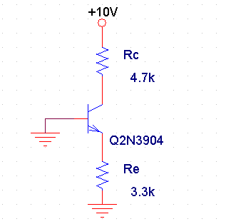
The solution says:
"The collector-base junction cannot conduct, since the n-type collector is connected through Rc to the positive power supply while the p-type base is at ground. It follows that the collector current will be zero."
I don't really understand this explanation. I was under the impression that for a transistor in active mode, Vc > Vb so CB junction is reverse biased, which is the case in this example.
What am I missing? Thank you.
The solution says:
"The collector-base junction cannot conduct, since the n-type collector is connected through Rc to the positive power supply while the p-type base is at ground. It follows that the collector current will be zero."
I don't really understand this explanation. I was under the impression that for a transistor in active mode, Vc > Vb so CB junction is reverse biased, which is the case in this example.
What am I missing? Thank you.