bjt amplifier basic.......

Thread Starter

Zeeus

Joined Apr 17, 2019
616
Should have done this yesterday :( sleep took over = not a true intellectual

Someone please assist :

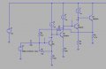
Due to R4 and R5, difference between emitter of Q3 and Q1 is about 5.6v..Emitter of Q3 be 6v and Q1 400mv (1mA which is same as 1mA on Q1's collector)

Since 1mA at Q2, it's base about 1.7V..Problem is that emitter of Q3 is about 10.5v..Like Q2 is cut off


Made a simpler circuit by omitting Q2 and everything checks out..gain was about 100 due to current source on Q1

Just want to add another amplifier to test understanding

Assist please..input impedance is problem?

Thanks


Edit : 2 questions actually ..Similar to this i guess
https://forum.allaboutcircuits.com/threads/bjt-resistive-divider-biasing.160181/

for R4 and R5
1. R4 =7.5k R5 = 1.2k
2. R4 = 68k and R5 = 10k
3. R4 = 750k R5 = 110k

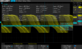
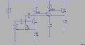
Using these 3 and simpler circuit, omitting Q2 with no current source on collector of Q1 and using 5.1k as collector resistor

emitter of follower = E
gain = G

1. E = 5.4v G = 9
2. E = 5.9V G = 11
3. E = 8.2V G = 9.2

Seems using 2, 68k and 10k was the best...How to know which to use ??

Thanks thanks
 

Attachments

Last edited:

Jony130

Joined Feb 17, 2009
5,488
What if to add another amplifier..so there are 3 common emitter transistors?
Cascading more than 3 stages of a CE amplifier is not a good idea. This is asking for trouble, the amplifier may turn into an oscillator due to additional phase shifts introduced by each stage.
 

Thread Starter

Zeeus

Joined Apr 17, 2019
616
Cascading more than 3 stages of a CE amplifier is not a good idea. This is asking for trouble, the amplifier may turn into an oscillator due to additional phase shifts introduced by each stage.
Thanks...Will give it a try soon to see

but no coupling though, except in beginning input and maybe output but no output cap yet
 

Thread Starter

Zeeus

Joined Apr 17, 2019
616
Thinking current will not flow through emitter of Q1 but it can flow through R4 and R3?


Will simulate


Trying to do the 3 stage amplifier

Edit :
Understand now (guess)...Thanks!! This formation not in current book reading

Voltage at Q1, sets output dc voltage...Emitter to emitter
Emitter of Q1 is fixed (10- Vbe)

Thanks Jony..will build later...Another circuit

Like this too
https://forum.allaboutcircuits.com/threads/basic-transistor-diff-amp.159887/#post-1394708

you fixed collector voltage of first transistor

but why keep base of Q1 at 10v? 7.5V maybe so output has about 6V dc ?
 
Last edited:

Jony130

Joined Feb 17, 2009
5,488
Thinking current will not flow through emitter of Q1 but it can flow through R4 and R3?
Yes, the DC Q1 emitter current will flow through R4 and R3.

you fixed collector voltage of first transistor
but why keep base of Q1 at 10v? 7.5V maybe so output has about 6V dc ?
If I understand your question correctly you must note that the voltage at Q1 collector is fixed by Q2 Vbe voltage (PNP).
Additional notice that Q2 is a PNP stage that provides an "active DC level shifting", now the output voltage at Q2 collector is now at ground reference.

More about this here (voltage “stacking”):
https://wiki.analog.com/university/...t/chapter-10#dc_coupled_common_emitter_stages
https://wiki.analog.com/university/courses/electronics/text/chapter-10#complementary_pair_amplifier
 

Thread Starter

Zeeus

Joined Apr 17, 2019
616
Did the 3 stage amplifier
Q1 TIP41

Dc voltage calculation to set V output as 6v worked..

oscillation : Why is this?? adding 0.1u to cap of Q3 ONLY, reduces the frequency of the oscillation but it is still there (with large amplitude, without connecting signal)

Amplifier not good : checked wiring, not sure wiring problem : not good on spice too

Anyways..Thanks ..can start day now
 

Attachments

Thread Starter

Zeeus

Joined Apr 17, 2019
616
Additional notice that Q2 is a PNP stage that provides an "active DC level shifting", now the output voltage at Q2 collector is now at ground reference.

More about this here (voltage “stacking”):
https://wiki.analog.com/university/...t/chapter-10#dc_coupled_common_emitter_stages
https://wiki.analog.com/university/courses/electronics/text/chapter-10#complementary_pair_amplifier
"now the output voltage at Q2 collector is now at ground reference. " don't understand this

but I know you mean Q3 and not Q2

Thanks for links
 

Thread Starter

Zeeus

Joined Apr 17, 2019
616
You can play with this circuit
Series feedback :) This setup better than book own

Output in phase with input so you send output to emitter so Vbe reduces as Vb increases..correct?

Anyways, here..Struggled with this for some time...lol but it works on spice :(

The base is about 7.5V so expect emitter to be about 6.8v but emitter is about 11.8V which is weird (spice has about 6.8)
Because of 100u so expect collector of Q2 to be about 5.8v
Goal was to change the 100 ohms later to 10 ohms to get gain of 1000 but this like this, DC point not what to expect

what can be a problem with circuit? checked connection, current sources working fine..dunno

See if any problem that will not make it work
 

Attachments

Thread Starter

Zeeus

Joined Apr 17, 2019
616
In real life, what did you use for I1 and I2?
I used two transistors each for current source..Just changed the I2 to three transistors but still not working!!!

Frustrating..base of Q1 is 7.5V but it's emitter is about 11v

Will attach the current source...Please look

Thanks
 

Thread Starter

Zeeus

Joined Apr 17, 2019
616
Seems to be working..dunno what's wrong

Base of Q1 is about 7.5V but emitter is about 11v..what can be the problem?

I removed everything and did again, cross checked more than 3 times..Not sure wiring problem

and its transistor IC for all transistors...ca3096
 

Attachments

Thread Starter

Zeeus

Joined Apr 17, 2019
616
Good good...Spice and I are getting same thing..This image here is what i have...Notice change on Q4....collector to base

Now base is 7.5V but emitter is 11.9V..

Good job spice :) :)

why remove the collector to base wire on Q4? (removing it then it works on spice : will try on breadboard) but why remove? needed for current source
 

Attachments

Bordodynov

Joined May 20, 2015
3,181
amp2.png amp1.png It is quite possible to use three stages of a circuit with a common emitter, if we introduce into them several negative feedbacks. As a bonus, this is a more stable gain and reduced distortion. Here is an example of such an amplifier:
 

Attachments

Last edited:

Jony130

Joined Feb 17, 2009
5,488
Good job spice :) :)
No, is a typical exampel of a GIGO. Answer yourself this question. What is the path for a base current for Q4 and Q3 if you disconnect the wire between Q4 base and collector?
Why did you decide to use a current mirror in the first place? What is the benefit here? Do you understand what consequence it will bring on the circuit operation? And then you expected that this circuit will work in real life?
 

Thread Starter

Zeeus

Joined Apr 17, 2019
616
It is quite possible to use three stages of a circuit with a common emitter, if we introduce into them several negative feedbacks. As a bonus, this is a more stable gain and reduced distortion. Here is an example of such an amplifier:
Understand circuit a bit....
COllector of Q3 is (246/36)*0.7 V..then can find it's emitter current then can calculate dc point of every other transistor
gain without C1 210/7.5

but somehow C1 increases gain, don't understand how

And kindly post any transistor circuit :D

Edit : so the bypass caps C2 and C3 help in anyway to reduce oscillation? cause did 3 stage amplifier like this and there was oscillation : would attempt this after understanding

Edit : oh see now (guess)...C1 provides negative feedback!!! Collector of Q3 increases as base of Q2 increases so you send output to the emitter!!!!! so as Vb increases, Ve increases too...Yeah?

God bless you! Post another circuit!

Missed anything?
 

Attachments

Last edited:

Thread Starter

Zeeus

Joined Apr 17, 2019
616
No, is a typical exampel of a GIGO. Answer yourself this question. What is the path for a base current for Q4 and Q3 if you disconnect the wire between Q4 base and collector?
lol, no path for it to flow..what is GIGO?

Why did you decide to use a current mirror in the first place? What is the benefit here? Do you understand what consequence it will bring on the circuit operation? And then you expected that this circuit will work in real life?
Used current source so high impedance and high open loop gain...Enlighten me professor Jony..what to do? why current mirror will not work? I've used current source with two transistors for the other kind of feedback more than 3 times (not series feedback) and works without trouble

Why not work now? when it will work? Post transistor circuit
 
Top