Facebook
 Google
 GitHub
 Linkedin
I am reading about average current mode control of switching power supply from this application note.
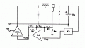
In the example 1 of the app note, the author said "Near fs, the amplifier gain is flat. The overall current loop has only one active pole (from the inductor)." Can anyone help me to understand it intuitively and quantitatively?


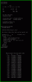
For the current compensation in red box, I derived the transfer function as below:

However, I don't know how to arrive at the conclusion given above.
In the example 1 of the app note, the author said "Near fs, the amplifier gain is flat. The overall current loop has only one active pole (from the inductor)." Can anyone help me to understand it intuitively and quantitatively?
For the current compensation in red box, I derived the transfer function as below:
However, I don't know how to arrive at the conclusion given above.


")