I saw ads for GaN chargers and dug a little on the web. Does anyone here know about GaN components? like what are the transistors like? do they make FETs, diodes, Zeners etc out of this material?
I have used many different types of GaN MOSFETs and Junctions GaN FETs. During the early stages there were too many types and the worst dies out. LOL
I don't think there are GaN Zeners.
I have used MOSFETs as diodes.
Most of the GaN MOSFETs are very fast switching, low capacitance, parts that have a very small Gate Turn On voltage. IF you are using the Transistor at 1mhz you really don't want to drive the Gate at 15 or 20V. Many of the GaN parts have a 5V or 6V Gate Breakdown voltage. Normal Gate Drivers do not work at 2 to 4V.
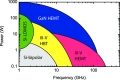
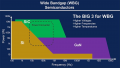
There are a bunch of graphs like this floating around, and they're generally pretty accurate, though most underestimate the frequencies to which GaN devices operate.
The long and short of it is this: low-frequency GaN is nearly competitive with SiC for power switching applications, though SiC remains the king of high voltage due to the enormous breakdown fields (though GaN is no slouch - 100V or higher GaN does exist from some companies). For RF applications, GaN is the current leading technology when measuring combined metrics like \(f_t\) and power density, and has breakdown voltages exceeding 50V (though 25V or 28V is more common to see) into the tens of GHz, depending on the particular foundry process. I've designed into a few of these processes, for both low- and high-frequency applications, as well as low- and high-power (and efficiency) applications.
Most GaN (or AlGaN, as most seem to be anymore) HEMTs are generally n-type, if I'm not mistaken, and usually are depletion-mode, though enhancement-mode GaN devices do exist.
GaN is also used for SB diodes, blue LEDs, and lasers. I think @ronsimpson is correct regarding zeners.
High-frequency AlGaN still struggles against (non-permanent) electron trapping effects, but not nearly as badly as 20+ years ago, as far as I know.
As far as chargers being advertised as being specifically GaN, that's mostly marketing, in my opinion. A lot of power converters use either GaN or SiC nowadays (except low-power ones which may still use Si devices), so calling it out as being a "GaN charger" is just fluff.
View attachment 369088View attachment 369089
There are a bunch of graphs like this floating around, and they're generally pretty accurate, though most underestimate the frequencies to which GaN devices operate.
The long and short of it is this: low-frequency GaN is nearly competitive with SiC for power switching applications, though SiC remains the king of high voltage due to the enormous breakdown fields (though GaN is no slouch - 100V or higher GaN does exist from some companies). For RF applications, GaN is the current leading technology when measuring combined metrics like \(f_t\) and power density, and has breakdown voltages exceeding 50V (though 25V or 28V is more common to see) into the tens of GHz, depending on the particular foundry process. I've designed into a few of these processes, for both low- and high-frequency applications, as well as low- and high-power (and efficiency) applications.
Most GaN (or AlGaN, as most seem to be anymore) HEMTs are generally n-type, if I'm not mistaken, and usually are depletion-mode, though enhancement-mode GaN devices do exist.
GaN is also used for SB diodes, blue LEDs, and lasers. I think @ronsimpson is correct regarding zeners.
High-frequency AlGaN still struggles against (non-permanent) electron trapping effects, but not nearly as badly as 20+ years ago, as far as I know.
As far as chargers being advertised as being specifically GaN, that's mostly marketing, in my opinion. A lot of power converters use either GaN or SiC nowadays (except low-power ones which may still use Si devices), so calling it out as being a "GaN charger" is just fluff.
Thanks, very interesting, hardly really heard about this until recently, back when I was in college and more up to date, everyone was excited about Gallium Arsenide if I recall, I have no recollection (1970s) of Gallium Nitride being a "thing".
If GaN switches so fast why isn't being used in computing?
The most fundamental issue is that there are no p-type GaN devices (or, at least, no p-type GaN devices that are currently in production - mostly only in research labs as far as I know). As it turns out, getting GaN to function with p-type materials is incredibly hard. Hypothetically, you could make "ye-olde-fashioned" nmos logic, but that's if there were no other issues.
GaN also has a bunch of other issues that make it ill-suited for computing. First, they're primarily high-power devices; their IV curve knees tend to be at several volts. Second, they're "normally-on" devices - they take a negative voltage to force them off. Third, they're massive compared to what we've got in silicon (though comparable to what was available in the 90s/early 200s). For instance: a lot of MACOM's (formerly Wolfspeed's) GaN devices are 250nm devices; some bigger, some smaller. That's a general trend of a lot of GaN transistors as well - generally 150nm or bigger gate sizes, though there are a few 90nm devices out there and sparingly few smaller.
Off the top of my head, I don't know what the Ion/Ioff ratio is, but I don't think it's as good as silicon transistors at the moment (you've got leakage).
Finally, the charge-trapping effects have the potential to cause problems down the line. In a "hand-wavy" kind of way, it would appear as a variation on latchup/latchdown that requires strong voltages to clear the traps. In RF or power devices, this leads to "current collapse," where your drain current suddenly drops, if I recall right.
GaN was only starting to be "a thing" in the 90s, if I recall my history right (may have been earlier, but not much), but didn't really start making a true industrial difference until the 2010s when a lot of the early GaN problems were resolved. At that time, "everyone" thought SiC would be the "next big thing," but it just couldn't keep up with GaN for high-frequency applications. By moving from GaN-on-Si to GaN-on-SiC and using AlGaN instead of pure GaN, a lot of lithography and manufacturing problems were resolved, if I recall right, as well as a few device-specific issues (charge trapping used to be a much worse problem). GaAs is still a big thing if you want low noise RF applications - most low-noise amplifiers I'm aware of use GaAs, but there are some features of GaN that, despite it having more noise than GaAs, offer some benefits GaAs does not have (such as power handling/survivability).
And while I'm thinking of novel transistors that make the rounds every so often, I'll add: there's a bunch of 2D transistor technologies that occasionally make the news as being the "next holy grail of computing" that probably won't go anywhere. Carbon nanotube FETs, graphene and graphene nanoribbon FETs (GFETs and GNRFETs, respectively), and, more recently, molybdenum sulfide FETs (MoS2 FETs - not sure if that's the official name of them or not) have all been posited to be the "next big thing," but all suffer manufacturing problems that make them impractical unless there's some industrial revolution. GNRFETs, for instance, have been "a thing" for probably close to 20 years now, promising transition frequencies in the THz(!!) range (with the highest number I saw being ~15 THz) and operating at even lower voltages than silicon devices (~1V max) and are pretty thermally stable (with undegraded performance being measured down to 4K, and barely generate heat because graphene is highly thermally conductive and the device pulls microwatts of power) and have equal charge mobilities for p-type and n-type devices (so the PFETs and NFETs can be the same size, unlike silicon), with pretty comparable Ion/Ioff ratios to silicon. However, they remain lab-only novelty devices, as you need to be able to line up a few pristine ribbons of graphene, each 12 or fewer atoms wide (I think they can go up to 16 or so before they stop being considered "nanoribbons" - that's a very important detail for these), in a particular orientation, over the length of 15nm, with near-perfect spacing between each ribbon, on perfectly-flat substrate material (Si, SiC, HfO2, sapphire, etc), with both a top- and bottom-gate structure to control the electric fields properly. One lab-grade sample (a "hero" or "golden sample") is hard enough to produce; imagine billions. Any deviation from perfection and your transistor, if it functions, is severely degraded.
Not particularly relevant to your original question, but it's worth noting as an interesting addendum to my prior answer, I think.
The most fundamental issue is that there are no p-type GaN devices (or, at least, no p-type GaN devices that are currently in production - mostly only in research labs as far as I know). As it turns out, getting GaN to function with p-type materials is incredibly hard. Hypothetically, you could make "ye-olde-fashioned" nmos logic, but that's if there were no other issues.
GaN also has a bunch of other issues that make it ill-suited for computing. First, they're primarily high-power devices; their IV curve knees tend to be at several volts. Second, they're "normally-on" devices - they take a negative voltage to force them off. Third, they're massive compared to what we've got in silicon (though comparable to what was available in the 90s/early 200s). For instance: a lot of MACOM's (formerly Wolfspeed's) GaN devices are 250nm devices; some bigger, some smaller. That's a general trend of a lot of GaN transistors as well - generally 150nm or bigger gate sizes, though there are a few 90nm devices out there and sparingly few smaller.
Off the top of my head, I don't know what the Ion/Ioff ratio is, but I don't think it's as good as silicon transistors at the moment (you've got leakage).
Finally, the charge-trapping effects have the potential to cause problems down the line. In a "hand-wavy" kind of way, it would appear as a variation on latchup/latchdown that requires strong voltages to clear the traps. In RF or power devices, this leads to "current collapse," where your drain current suddenly drops, if I recall right.
GaN was only starting to be "a thing" in the 90s, if I recall my history right (may have been earlier, but not much), but didn't really start making a true industrial difference until the 2010s when a lot of the early GaN problems were resolved. At that time, "everyone" thought SiC would be the "next big thing," but it just couldn't keep up with GaN for high-frequency applications. By moving from GaN-on-Si to GaN-on-SiC and using AlGaN instead of pure GaN, a lot of lithography and manufacturing problems were resolved, if I recall right, as well as a few device-specific issues (charge trapping used to be a much worse problem). GaAs is still a big thing if you want low noise RF applications - most low-noise amplifiers I'm aware of use GaAs, but there are some features of GaN that, despite it having more noise than GaAs, offer some benefits GaAs does not have (such as power handling/survivability).

 Facebook
 Google
 GitHub
 Linkedin