AND gate issue

Thread Starter

wchris777

Joined Dec 1, 2018
13
Hello there,

I buit this simple AND gate :

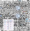
but unfortunately it doesn't perform as I expected.
First, I was always told to never connect the load to the NPN emitter pin. Does anyone know why it's the case in this schematics?
Second, whenever the B port is high, the OUT port is high too.
My setup is the following: VCC is 5V, A and B are driven by PIR detectors that output 3.3V. R is 4.7K and the NPN transistors are 2N2222.
Now, when only A is high, OUT is down.
when A and B are high, OUT is high (2.8V)
when B is high and A is down, OUT is high (2.2V)

Does anyone know what is wrong with this gate?
Thank you.
 

Attachments

JSCV

Joined Oct 3, 2015
23
A current can still flow from base to emitter on the port B input, even if port A = 0
Depending on your resistor ratio there could be enough voltage over R2 to drive your output Q
 

dl324

Joined Mar 30, 2015
16,943
First, I was always told to never connect the load to the NPN emitter pin. Does anyone know why it's the case in this schematics?
Whoever told you that was wrong. You can't make an AND gate without stacking the transistors.
Second, whenever the B port is high, the OUT port is high too.
The output should be LOW until both inputs are HIGH.
My setup is the following: VCC is 5V, A and B are driven by PIR detectors that output 3.3V. R is 4.7K and the NPN transistors are 2N2222.
Now, when only A is high, OUT is down.
when A and B are high, OUT is high (2.8V)
when B is high and A is down, OUT is high (2.2V)
You're complicating things by introducing a level shift.

When B is HIGH and A is LOW, the output should be LOW. Measure voltages at each node until you find the one that's wrong. That will give you a clue as to what is malfunctioning.
 

ebp

Joined Feb 8, 2018
2,332
If the upper transistor is off, the lower one cannot operate as a normal transistor because there is no source of current into the collector. In that case, the base-emitter junction simply behaves as a diode and the emitter voltage will be about 0.7 V less than the base voltage. The actual voltages at the base and emitter then become a function of the voltage applied at the B input, this voltage drop and the resistors, calculated using Kirchhoff's voltage law and Ohm's law.
 

Thread Starter

wchris777

Joined Dec 1, 2018
13
If the upper transistor is off, the lower one cannot operate as a normal transistor because there is no source of current into the collector. In that case, the base-emitter junction simply behaves as a diode and the emitter voltage will be about 0.7 V less than the base voltage. The actual voltages at the base and emitter then become a function of the voltage applied at the B input, this voltage drop and the resistors, calculated using Kirchhoff's voltage law and Ohm's law.
I think you have a point. T2 acts indeed as a diode when T1 is off as the voltage across T2 is ~0.7V
Is there any way to make this gate work? I have the impression that it's design is wrong.
 

crutschow

Joined Mar 14, 2008
34,470
Is there any way to make this gate work?
You can increase the value of the base resistor relative to the emitter resistor value.
Depending upon the gain of the transistors you could likely make the base resistors 50 to 100 times the emitter resistor.
That will make the ghost output voltage small compared to the normal logic-high output voltage.
 

ebp

Joined Feb 8, 2018
2,332
As Albert (and crutschow, as I was typing) suggested, changing the resistors may help.

There are alternative ways to make an AND gate using diodes, provided that the input sources can "sink" current when LOW (often the case, and in fact the sinking ability may exceed sourcing). To "sink" current means to conduct "conventional current", which is regarded as flowing from positive to negative, in this case to the circuit "common" or "ground."

The simplest circuit consists of two diodes with their anodes connected together and a "pullup" resistor from the anodes to the positive supply (which should be the same voltage as the HIGH output voltage from the inputs to avoid possibly applying excessive voltage to the input circuits) - this node is the output. If either input is low, the output is LOW (but at least a diode drop above ground). If both inputs are HIGH then the output is HIGH. For some applications, this is quite satisfactory, for others it isn't. You could add an emitter follower (common collector) stage for higher output current sourcing ability, or two common-emitter inverter stages for good current sinking ability. In terms of parts count and board area, using discrete components can be a poor tradeoff against a DIP IC gate package in which you only use 1 or 2 gates, and certainly against a single surface mount gate in SOT-23 or smaller package.
 

ebp

Joined Feb 8, 2018
2,332
I should have mentioned:

Sometimes outputs of devices use transistors to drive LOW and resistors to pull the output HIGH. If that is what you have, you can directly connect the outputs together (with some caution with regard to positive supply - it can be a problem if one device has power and the other doesn't) to make a "wired-AND" configuration.
 

Thread Starter

wchris777

Joined Dec 1, 2018
13
You can increase the value of the base resistor relative to the emitter resistor value.
Depending upon the gain of the transistors you could likely make the base resistors 50 to 100 times the emitter resistor.
That will make the ghost output voltage small compared to the normal logic-high output voltage.
Yes I confirm that works. I just had to adjust the R resistor on T2 to get the output lower than the IC's external interrupt voltage threshold.
If both A and B are high the output voltage is above the threshold and if only B is high, the output voltage is below the threshold. This doesn't look like a perfect solution but still it works as expected in my circuit.
Thank you very much guys for your help. I really appreciate that.
 

Thread Starter

wchris777

Joined Dec 1, 2018
13
Well that works but this solution is limited. If I want to plug an LED to this gate's output in addition to the IC's input, I would have to re-adjust the resistor values. Now if the LED burns or whatever, the resistors would have to be re-adjust again and whole system wouldn't recover by itself.
I can't use this gate for my project. I tried to use MOSFETs instead of BJT transistors as they are voltage driven but I get the same issue with the middle transistor turning the gate's output high despite the value of the second input...

Is it even possible to build an AND gate using transistors that's output is exactly VCC (5V) when the two inputs are high and exactly 0V when one of them is low?
Thanks for your help.
 

dl324

Joined Mar 30, 2015
16,943
Well that works but this solution is limited. If I want to plug an LED to this gate's output in addition to the IC's input, I would have to re-adjust the resistor values.
Post a schematic with the values you ended up using.
Is it even possible to build an AND gate using transistors that's output is exactly VCC (5V) when the two inputs are high and exactly 0V when one of them is low?
That isn't how TTL works, so why would you care if the outputs weren't an exact voltage? All logic families have a range of values that are considered HIGH and LOW.
 

Thread Starter

wchris777

Joined Dec 1, 2018
13
Post a schematic with the values you ended up using.
That isn't how TTL works, so why would you care if the outputs weren't an exact voltage? All logic families have a range of values that are considered HIGH and LOW.
R=10K, R2=4.7K With these I get an output of: 0V when A&B are down, 0.9V when B is high and 2.2V when A&B are high. (A and B are at 3.3V when high).
What I need is to have an output of 0V when one of them or both are low and an output of at least 3V when both of them are high. Is that possible?
 

AlbertHall

Joined Jun 4, 2014
12,347
R=10K, R2=4.7K With these I get an output of: 0V when A&B are down, 0.9V when B is high and 2.2V when A&B are high. (A and B are at 3.3V when high).
What I need is to have an output of 0V when one of them or both are low and an output of at least 3V when both of them are high. Is that possible?
Yes, it's possible but it will be more complictaed than just two transistors.
 

dl324

Joined Mar 30, 2015
16,943
R=10K, R2=4.7K With these I get an output of: 0V when A&B are down, 0.9V when B is high and 2.2V when A&B are high. (A and B are at 3.3V when high).
What I need is to have an output of 0V when one of them or both are low and an output of at least 3V when both of them are high. Is that possible?
What is the voltage at the emitter of T1 when both inputs are HIGH?

You should use LOW instead of down. Logic levels are HIGH and LOW or 1 and 0, but not up or down.
 
Top