Analog Intresting circuit help needed

Thread Starter

mishra87

Joined Jan 17, 2016
1,034
Hey Guys,
I am trying to understand below circuit and how this circuit works any help here is highly appreciated.

Any simulation in ltspice will be really helpful.

Assumption.
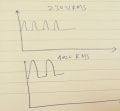
My input is 230Vrms so output should high
if input is 400Vrms output is low.

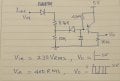
Here is circuit i have drawn in copy.

Humble Thanks in Advance !
M
 

Attachments

Papabravo

Joined Feb 24, 2006
21,225
For 230 VRMS, \( V_{pk}\;=\;230\text{ Vrms}\times\sqrt{2}\;\approx\;326\text{ V} \)
Similarly 400 VRMS, \( V_{pk}\;=\;400\text{ Vrms}\times\sqrt{2}\;\approx\;566\text{ V} \)
Neglecting the voltage drops of the diode, compute the voltage at the junction of the voltage divider when the AC waveform reaches the peak voltage.
\( V_{d230}\;=\; 326\times\cfrac{10}{1186}\;=\; 2.75 \text{ V} \)
\( V_{d566}\;=\; 566\times\cfrac{10}{1186}\;=\; 4.77 \text{ V} \)

Do those two numbers give you a clue
 
Last edited:

Thread Starter

mishra87

Joined Jan 17, 2016
1,034
For 230 VRMS, \( V_{pk}\;=\;230\text{ Vrms}\times\sqrt{2}\;\approx\;326\text{ V} \)
Similarly 400 VRMS, \( V_{pk}\;=\;400\text{ Vrms}\times\sqrt{2}\;\approx\;566\text{ V} \)
Neglecting the voltage drops of the diode, compute the voltage at the junction of the voltage divider when the AC waveform reaches the peak voltage.
\( V_{d230}\;=\; 326\times\cfrac{10}{1186}\;=\; 2.75 \text{ V} \)
\( V_{d230}\;=\; 566\times\cfrac{10}{1186}\;=\; 4.77 \text{ V} \)

Do those two numbers give you a clue
Hey thanks for support.
I did this calculation on paper and my perception was.

1. When divider voltage is 2.7V
2.7+Vd = 2.7+0.8V =3.5V
considering the voltage drop across diode is 0.8V
since 3.5<5 , PNP will conduct and output of pnp Vo = 5V

2. 4.7V+0.8V=5.5V
5.5V>5V so pnp will not conduct.

Now since 2.7V and 4.7V is not pure DC so in this case what will happen.

peak 0-2.7V , pnp will always ON
peak 4.7V, from peak 0V-4.3V pnp will ON and from 4.3V-4.7V pnp will be off.
so this we have high and low signal at output.

Thats what i understood.

Now i see there is dc shift at divider point and i dont know why signal at this point not starts from 0V.
attachment shows two different image for 230V and 400V. 230V have small deltaX while 400v have more deltaV

Lets wait if someone try to simulate and shows, sorry at the moment at i dont have access of simulation tool.

thanks again for your intrest.
 

Attachments

Papabravo

Joined Feb 24, 2006
21,225
Here is the simulation. As you can see, the output is not the square wave you might have expected. When Vbe ≥ -0.7 VDC, transistor Q1 turns off momentarily, allowing the pull-down resistor to take Vo lower than its nominal value of about 5 volts. A smaller value than 10K for R4 might get you a more useable waveform.
1667681672818.png
You can rename the .txt file as a .plt file to reproduce the waveforms.
 

Attachments

Thread Starter

mishra87

Joined Jan 17, 2016
1,034
Here is the simulation. As you can see, the output is not the square wave you might have expected. When Vbe ≥ -0.7 VDC, transistor Q1 turns off momentarily, allowing the pull-down resistor to take Vo lower than its nominal value of about 5 volts. A smaller value than 10K for R4 might get you a more useable waveform.
View attachment 280018
You can rename the .txt file as a .plt file to reproduce the waveforms.
Hey P,
Many thanks for your simulation.
below things i would like to ask you. Sorry i do not have ltspice access at the moment.
1. i see your divider output start from 4.2V, why ?
2. your Vo swing from 5V to 2.4V not 0V, why ?
3. how pnp works ?
Ve = 5v
Vb should be 0.7V below Ve menas if Vb=4.3V, pnp should work isn't it ?
4. what is use of D2 diode in circuit?
Against a big Thanks to you !
M
 
Last edited:

WBahn

Joined Mar 31, 2012
30,052
I'd recommend focusing your attention on understanding the right half of the circuit and how to analyze it.

Also, I'm hoping that you are only playing with this circuit in simulation, and not actually building it. Mixing high-voltage and low-voltage circuits is extremely risky unless you are very careful AND have a good understanding of what you are doing and how to work with high-voltage circuits.
 

Papabravo

Joined Feb 24, 2006
21,225
Hey P,
Many thanks for your simulation.
below things i would like to ask you. Sorry i do not have ltspice access at the moment.
1. i see your divider output start from 4.2V, why ?
2. your Vo swing from 5V to 2.4V not 0V, why ?
3. how pnp works ?
Ve = 5v
Vb should be 0.7V below Ve menas if Vb=4.3V, pnp should work isn't it ?
4. what is use of D2 diode in circuit?
Against a big Thanks to you !
M
  1. The voltage divider always has the same ratio. That is 10K/(1176K +10K) = 8.43E-03. The actual voltage will depend on the current through D2.
  2. The time where the transistor is off is very short, and the voltage does not have time to get all the way to ground. I mentioned this in post #4 just above the simulation. Do you read what I write, or do you just look at my posts for the pictures?
  3. A PNP woks the opposite of an NPN. Vbe needs to be negative to turn the transistor on. that is Vb must be about 0.7 volts below Ve. It meets that condition most of the time. The high voltage input reduces Vbe to a larger negative value and turns the transistor off very briefly and so Vo heads for GND via R4.
  4. D2 prevents any large positive voltage from affecting R3, D3, R4, and Q1.
Although the simulation shows the logic ground and the AC ground at the same potential. A real circuit should not be built like this. Pay head to the warning in post #6.
 

Thread Starter

mishra87

Joined Jan 17, 2016
1,034
  1. The voltage divider always has the same ratio. That is 10K/(1176K +10K) = 8.43E-03. The actual voltage will depend on the current through D2.
  2. The time where the transistor is off is very short, and the voltage does not have time to get all the way to ground. I mentioned this in post #4 just above the simulation. Do you read what I write, or do you just look at my posts for the pictures?
  3. A PNP woks the opposite of an NPN. Vbe needs to be negative to turn the transistor on. that is Vb must be about 0.7 volts below Ve. It meets that condition most of the time. The high voltage input reduces Vbe to a larger negative value and turns the transistor off very briefly and so Vo heads for GND via R4.
  4. D2 prevents any large positive voltage from affecting R3, D3, R4, and Q1.
Although the simulation shows the logic ground and the AC ground at the same potential. A real circuit should not be built like this. Pay head to the warning in post #6.
Thanks for your clarification !
Warning : If you look at my post #1 the circuit i used was Line connected to some other GND and not with Neutral.

i read the explanation of point 1 of this post.
sorry to say i still do not understand why vd start from 4.2V ?
For 325V peak , vd = 2.7V peak
from another loop of 5V ,vd would be 4.2V (5v-diode d2 drop).
Now if both signal super imposed where 2.7V peak voltage goes.
"The actual voltage will depend on the current through D2." what does it mean ?
sorry asking again may be silly question.
thanks for help.
 

Papabravo

Joined Feb 24, 2006
21,225
Thanks for your clarification !
Warning : If you look at my post #1 the circuit i used was Line connected to some other GND and not with Neutral.

i read the explanation of point 1 of this post.
sorry to say i still do not understand why vd start from 4.2V ?
For 325V peak , vd = 2.7V peak
from another loop of 5V ,vd would be 4.2V (5v-diode d2 drop).
Now if both signal super imposed where 2.7V peak voltage goes.
"The actual voltage will depend on the current through D2." what does it mean ?
sorry asking again may be silly question.
thanks for help.
It is KCL for the node Vd.

\( \cfrac{V_{pk}-V_{d}}{1175\text{ kΩ}}+\cfrac{V_{d}}{10\text{ kΩ}}+I_{D2}\;=\;0 \)

Clearly this voltage will be different than the voltage with just R1 & R2
 
Top