 Facebook
 Google
 GitHub
 Linkedin
Hello everyone,
This is my first time posting here.
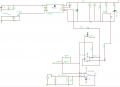
I’m a new student in electronics engineering, and I’m helping to improve a circuit design.
The original design is a bit confusing, and I need your help to understand what the circuit is supposed to do.
I’ll share what I know about the design and hope you can help me figure out the parts I don’t understand yet:
First, this is a DC-DC converter called the TPS5430 made by Texas Instruments.
Parameters:
V1=Vin = 24V
Vout should be 8.3V-8.7V
VG1 = 3.3V PWM (D.C.=95%-100%)
OP AMP VCC = 24V
OP AMP VDD = 0V (GND)
The 2 op amplifiers down the scheme are Less understandable to me.
I think OP2used as LPF and need your help for the OP1
Thanks!
simulated on TINE TI Scheme and transition result for 1 second running :


This is my first time posting here.
I’m a new student in electronics engineering, and I’m helping to improve a circuit design.
The original design is a bit confusing, and I need your help to understand what the circuit is supposed to do.
I’ll share what I know about the design and hope you can help me figure out the parts I don’t understand yet:
First, this is a DC-DC converter called the TPS5430 made by Texas Instruments.
Parameters:
V1=Vin = 24V
Vout should be 8.3V-8.7V
VG1 = 3.3V PWM (D.C.=95%-100%)
OP AMP VCC = 24V
OP AMP VDD = 0V (GND)
The 2 op amplifiers down the scheme are Less understandable to me.
I think OP2used as LPF and need your help for the OP1
Thanks!
simulated on TINE TI Scheme and transition result for 1 second running :
Attachments
-
 95.1 KB Views: 0
 -
 31.2 KB Views: 0
 -
 95.3 KB Views: 0


