Allow DIP components to overlay each other in Altium

Thread Starter

Vilius_Zalenas

Joined Jul 24, 2022
173
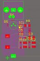
I am doing a board design in which I really need to minimize the PCB dimensions. I was wondering, if it is possible to allow the DIP components overlay each other on the top and bottom layers. I am doing some unique PCB, so I would grind the sticking pins of the PCB surface, dont worry about that... Thank you in advance.
 

Attachments

Papabravo

Joined Feb 24, 2006
21,225
I think it raises significant issues of testability and repairability. On the face of it sounds like a really bad idea. I suppose you gotta do you and potentially learn this the hard way.
 

Thread Starter

Vilius_Zalenas

Joined Jul 24, 2022
173
I think it raises significant issues of testability and repairability. On the face of it sounds like a really bad idea. I suppose you gotta do you and potentially learn this the hard way.
So there is no Altium PCB Rule option for this? Hmm, what if just generated the output files without DRC? The manufacturer should not be intimidated by this at all, the only job for the manufacturer is to manufacture the given files...
 

crutschow

Joined Mar 14, 2008
34,452
If you really need to minimize the board size that badly then go to smaller surface-mount devices.
They are a little harder to hand-solder but it can be done, and you will save a lot of space.
And it's not a problem to put the in the same area on each side of a double layer PCB.
 

ronsimpson

Joined Oct 7, 2019
3,037
components overlay each other on the top and bottom layers.
Not using Altium but.....
I make boards where the SMD are on the top and the through hole are on the other side. It is common for me to have the SMD top overlap the bottom parts. Much like when I have SMD on both sides.
I do not know Altium but.....
I have some parts where the part "keep out area" is on both sides of the board. Sorry I don't know what word you use. (Part outline)?? I some times have to edit a part so the DRC will allow me to place parts on the other side of the board.
I use large PCB transformers where I put diodes under the transformer on both sides of the board. I have to remove the keep_out area for the transformer.
 
Top