Advice on circumventing a +/-20V Vgs on a 24V Logic circuit

Thread Starter

ForgedAscendant

Joined Aug 26, 2017
6
Good Day,

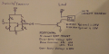
I had some issues with a control circuit I am putting together and you guys came together and gave me some really great tips on avoiding floating gates via pull down resisters. I implemented these ideas, revised my ideas to use the hardware available, and took a second look at a simplified circuit concept to isolate and eliminate problems. Below is a basic concept and the issue I found with it (this time I attempted to include all the relevant info):
upload_2017-8-29_21-52-17.png
The single FET on the Load side fails in the off state as the source rises to 24V while the gate remains at 0V creating a differential of 24V while the max allowable Vgs is 20V. I found this issue after reviewing the pull down resister concept and questioning why the load wouldn't behave in the same way. To prove this out practically, I took a multi-meter to it and found it to be 25.68V (Two 12V batteries connected in series) but for all intensive purposes; 24V.

I would greatly appreciate if someone could help me come up with a simple basic design for the above circuit to get around the Vgs problem? Once I have that, I can go on and apply the concept to the full circuit or if required redesign the entire thing.

Thank you for your time,
Forgedascendant
 

crutschow

Joined Mar 14, 2008
38,689
Since you didn't draw a standard MOSFET symbol (what exactly is that symbol :confused:) it's not completely clear to me how the circuit is connected, but if the N-MOSFET is switching the low side of the pump, then it's the drain that is going to 24V, not the source, and that's not a problem, since it's the Vgs that's of concern, not Vgd.
 

WBahn

Joined Mar 31, 2012
33,076
It would help quite a bit if you used the proper symbols on your schematics. You are (almost) using the symbol for a bipolar junction transistor (BJT). These behave very differently than field effect transistors (FET). Keep in mind that you are asking advice from people that, long ago, internalized these differences and may have a hard time not interpreting your circuit as using BJTs.

Also, there is a difference between an N-channel FET and between the source and drain terminals (and similar distinctions on a BJT), which is why the standard symbols not only distinguish between type of transistor (FET vs BJT), but what type of fet (N-channel FET vs P-channel FET) and which terminal is which (source vs drain). It will really help those trying to help you if you update your diagram accordingly.

This is important because it appears that part of your problem is that you are failing to recognize that the source and the drain are not interchangeable. From your notes it appears you are connecting the source of the transistor to the pump and connecting the drain to ground. That is backwards. Connect the drain to the pump and the source to ground, so that Vds (the voltage on the drain relative to the source) is positive.

Now your Vgs is the voltage between the gate and ground and this is the voltage you need to keep below 20 V. Since you are using a logic-level FET, there is no compelling reason to drive Vgs much above logic voltage levels of about 5 V and there are some reasons not to, though going up to 10 V or so should be any problems. Don't push the 20 V limit, unless you are willing to buy new transistors on a regular basis.

The solution to you problem is to simply use a voltage divider between your 24 V signal and the gate of the FET. Using two 1 kΩ resistors will drop Vgs to about 12 V, which should work fine. You could probably get by using a 33 kΩ for the top one and a 10 kΩ for the bottom one, which should give you a Vgs of about 5.6 V, which should be more than enough.
 

Thread Starter

ForgedAscendant

Joined Aug 26, 2017
6
It would help quite a bit if you used the proper symbols on your schematics. You are (almost) using the symbol for a bipolar junction transistor (BJT). These behave very differently than field effect transistors (FET). Keep in mind that you are asking advice from people that, long ago, internalized these differences and may have a hard time not interpreting your circuit as using BJTs.

Also, there is a difference between an N-channel FET and between the source and drain terminals (and similar distinctions on a BJT), which is why the standard symbols not only distinguish between type of transistor (FET vs BJT), but what type of fet (N-channel FET vs P-channel FET) and which terminal is which (source vs drain). It will really help those trying to help you if you update your diagram accordingly.

This is important because it appears that part of your problem is that you are failing to recognize that the source and the drain are not interchangeable. From your notes it appears you are connecting the source of the transistor to the pump and connecting the drain to ground. That is backwards. Connect the drain to the pump and the source to ground, so that Vds (the voltage on the drain relative to the source) is positive.

Now your Vgs is the voltage between the gate and ground and this is the voltage you need to keep below 20 V. Since you are using a logic-level FET, there is no compelling reason to drive Vgs much above logic voltage levels of about 5 V and there are some reasons not to, though going up to 10 V or so should be any problems. Don't push the 20 V limit, unless you are willing to buy new transistors on a regular basis.

The solution to you problem is to simply use a voltage divider between your 24 V signal and the gate of the FET. Using two 1 kΩ resistors will drop Vgs to about 12 V, which should work fine. You could probably get by using a 33 kΩ for the top one and a 10 kΩ for the bottom one, which should give you a Vgs of about 5.6 V, which should be more than enough.
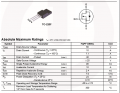
WBahn, thank you for responding and I will pay more attention to my drawings in the future and do a bit more research on proper figures before posting again. You are correct when you said I am interchanging source and drain. I took a look at the FET documentation posted below:
upload_2017-8-29_23-30-10.png
I looked at the published drawing (top right) and I see that the source and drain are both constructed in a similar manner (some sort of oxide ) so thus I concluded that If Vgs is limited to 20V then Vdg must be too. Is this a bad assumption on my part? If so, then I am happy to be wrong as the solution is exactly what you say and all I need to do is pay special attention to the drain and source when I try constructing the circuit again.
 

crutschow

Joined Mar 14, 2008
38,689
...and I see that the source and drain are both constructed in a similar manner (some sort of oxide )so thus I concluded that If Vgs is limited to 20V then Vdg must be too. Is this a bad assumption on my part?
Yes.
As it states in the data sheet, it's the Vgs voltage that's important, not Vgd.

The source and drain are not created with an oxide, it's the gate to the drain-source channel that is isolated with silicon oxide.
And the nature of the channel voltage distribution is such that the gate oxide sees the gate-source voltage, not the gate-drain voltage.
Thus the drain-source voltage is limited only by the drain-source (Vds) channel voltage rating.
 
Last edited:

WBahn

Joined Mar 31, 2012
33,076
I looked at the published drawing (top right) and I see that the source and drain are both constructed in a similar manner (some sort of oxide ) so thus I concluded that If Vgs is limited to 20V then Vdg must be too. Is this a bad assumption on my part? If so, then I am happy to be wrong as the solution is exactly what you say and all I need to do is pay special attention to the drain and source when I try constructing the circuit again.
Notice that the source is tied to the body of the channel. A FET is actually a four-terminal device. There is the silicon in which the source and drain are embedded and within which the channel forms. This is known as the body or the bulk. In a three-terminal device, the body is electrically connected to the source. Thus the gate source voltage also appears across the gate to body (across the thin oxide above where the channel forms) and too much voltage will destroy the oxide. The voltage between the gate and the drain doesn't appear across the thin oxide. Here the issue is the voltage between the source and the drain across the length of the channel region, and this can be quite a bit higher (as the data sheet shows).

Also notice that there appears to be an intentional diode between the source and drain, so if you connect it backwards it may not act like a transistor at all, but rather like a diode (and probably a pretty easily damaged one).
 

jayanthd

Joined Jul 4, 2015
945
See L298N datasheet. In its internal diagram it uses a resistor between low side sources and GND for sense pins. See if you can use a low ohm resistor to make a sense circuit which can be read using ADC of microcontroller.
 
Top