 Facebook
 Google
 GitHub
 Linkedin
PIC micro 18F2321
For several applications with ADC conversions I selected VREF- = Vss and VREF+ = Vdd, this last being 4,91V
Voltages to convert : 3,43V and 2,90V in AN0 and AN1 respectively. Conversion results were always correct:
For 3,43V I get 714
For 2,90V I get 604
Yesterday, changed to the option VREF+ = input in AN3. The actual external input is 3,69 V
Now, conversion results make no sense:
For 3,43V I get 1023
For 2,90V I get 1023
The input in AN3, is generated as shown in the image below. Calculated initially as 3,71V it is actually 3,69V
What am I doing wrong? Completely at lost here.

------------------------------------------------------------
Settings prior using the ADC module (LOADREG_IN_ACC is a macro):
For several applications with ADC conversions I selected VREF- = Vss and VREF+ = Vdd, this last being 4,91V
Voltages to convert : 3,43V and 2,90V in AN0 and AN1 respectively. Conversion results were always correct:
For 3,43V I get 714
For 2,90V I get 604
Yesterday, changed to the option VREF+ = input in AN3. The actual external input is 3,69 V
Now, conversion results make no sense:
For 3,43V I get 1023
For 2,90V I get 1023
The input in AN3, is generated as shown in the image below. Calculated initially as 3,71V it is actually 3,69V
What am I doing wrong? Completely at lost here.
------------------------------------------------------------
Settings prior using the ADC module (LOADREG_IN_ACC is a macro):
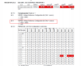
Code:
  LOADREG_IN_ACC  ADCON0,00000001B      ;ch.selection / enable module/ start
;                        0.......       XX
;                        .0......       XX
;                        ..0.....       channel
;                        ...0....       selection
;                        ....0...       while in
;                        .....0..       operation
;                        ......0.       don't GO yet - patience!
;                        ..... .1       ADC converter up and running

  LOADREG_IN_ACC ADCON1,00011011B       ;enabling analog channels and Vrefs
;                       0.......        XX
;                       .0......        XX
;                       ..0.....        =0 VREF- = Vss / =1 VREF- = input in AN2
;                       ...1....        =0 VREF+ = Vdd / =1 VREF+ = input in AN3
;                       ....1...        =1 enable
;                       .....0..        =0 channels
;                       ......1.        =1 0, 1, 2 & 3
;                       .......1        =1 as analog

  LOADREG_IN_ACC ADCON2,10010100B       ;format / acq time / converion clock
;                       1.......        =1 right justified
;                       .0......        XX
;                       ..0.....        =0 Tacq equal
;                       ...1....        =1 to
;                       ....0...        =0 4Tad
;                       .....1..        =1 Tad equal
;                       ......0.        =0 to
;                       .......0        =0 4 Tosc

;We set the four ADC pins as inputs

  BSF ADC_TRIS,0,A
  BSF ADC_TRIS,1,A
  BSF ADC_TRIS,2,A
  BSF ADC_TRIS,3,A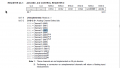

")


