Facebook
 Google
 GitHub
 Linkedin
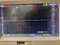
I have an analog Since wave signal that is centered at +2.5VDC and maxes out between 0-+5V. I need to adapt it to the analog read input pin of a 3.3VDC (around 10K-16K internal resistance) microcontroller (nRF52840). I built a voltage divider that moved the +2.5V center to +1.65VDC center (half of 3.3V), but I am still getting sine wave clippings at +4.5V and below zero volts (negative on the oscope).
So changed the voltage divider to center at +1.2VDC, which fixed the upper clippings to +2.88V, but looks like still getting negative clippings. I cannot change the source-setup of the 0-5V signal input, nor the 2.5V center. I can only modify that source signal.
Do I need to reduce the signal amplitude with an op amp to center it on +1.65V and limit the sine wave swings to stay within the 3.3V rail to prevent clippings? Any passive components fix or only op amp? I cannot do a software fix, because i need to capture the entire intact sine wave to do FFT on it.