AC amplifier, transistor with bias network

Thread Starter

electronicsenjoyer089

Joined Feb 24, 2025
182
Hello all, im trying to simulate and understand the circuit made with 4 resistors as bias network

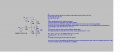
Now i explained each step in the image u can check below, but i will repeat here

So to start what i know is that i wanna make a voltage amplifier ( so in terms of current i dont care yet even if i dont know what i need to consider in order to make the amplifier actually work , so if u got any suggestion about what currents should flow in the circuit, tell me )

What i know is that VCC is 20V and VIN is 5VAC what i wanna obtain is a gain of AV=2, so in output i wanna have an ac voltage with 10v peak to peak

what i did is:
1° calculating R1 and R3 in order to set VB DC voltage, in this case i saw that the rule says it needs to be half of VCC, so R1=R3=10k
2° secondly i calculated the resistor on emitter, which i did by assuming IE=1mA ( this value i choose it? or i find it on datasheets? )
3° to choose RC i read there is another rule to have maximum signal swing, the midway beetwen 0 and 20V of VCC is 10V , so we wanna have VC = 10V

RC = (VCC - VC) / IC , for small currents IE=IC, so 1mA
In this case RC = 20 - 10 / 1*10^(-3) = 10k

4° and last step is double checking the gain AV=RC/RE = 10k/9.3 = 1,07 and we can see we dont obtain AV = 2 even if we followed the ''rules"

So i ask u, someone can help me clarifying my doubts? what i did wrong? what steps i need to follow? how i need to think whne building ac voltage amplifier ( current doesnt matter for me now )

Thanks and please use ''simple terms'' :D
 

Attachments

LvW

Joined Jun 13, 2013
1,999
@ electronicsenjoyer089

Just one general recommendation: Before starting such a design it would be very good if you at first would try to get a good and complete understanding of
(a) the transistors working principle and
(b) the role and the task of each of the 4 resistors.

(For example: Who has told you that Vb should be app 50% of Vcc?)

Without such a knowledge, you can, of course, make use of corresponding answers in this forum leading - more or less - to a "cookbook approch" . However, would this be for you really helpful?-
 

Thread Starter

electronicsenjoyer089

Joined Feb 24, 2025
182
@ electronicsenjoyer089

Just one general recommendation: Before starting such a design it would be very good if you at first would try to get a good and complete understanding of
(a) the transistors working principle and
(b) the role and the task of each of the 4 resistors.

(For example: Who has told you that Vb should be app 50% of Vcc?)

Without such a knowledge, you can, of course, make use of corresponding answers in this forum leading - more or less - to a "cookbook approch" . However, would this be for you really helpful?-
Hmm
(a) for working principle u mean that it acts as current controlled device? the internal diodes, and the general equations? like ic=hfe*ib for example?
(b) ye the first 2 resistors r1,r3 are used to set the voltage base (DC) , while the resistor RC is used to directly set the amplifier gain, limits collector current and it develops the output voltage swing since VC=VCC-IC*RC , so the signal on collector depends on RC

and as last the emitter resistor is used for thermal stability, for setting gain and provides negative feedback ( but i just know that theorically ) and as last it sets the emitter voltage clearly cus VE= IE*RE

am i missing something?
 

Thread Starter

electronicsenjoyer089

Joined Feb 24, 2025
182
@ electronicsenjoyer089

Just one general recommendation: Before starting such a design it would be very good if you at first would try to get a good and complete understanding of
(a) the transistors working principle and
(b) the role and the task of each of the 4 resistors.

(For example: Who has told you that Vb should be app 50% of Vcc?)

Without such a knowledge, you can, of course, make use of corresponding answers in this forum leading - more or less - to a "cookbook approch" . However, would this be for you really helpful?-
oh that thing of VB should be 50% of VCC i read it on a website, but im not sure.. other says u set emitter current then u find VE
and since VB=VE+VBE then u find VB but no idea if that is correct or not.
 

BobTPH

Joined Jun 5, 2013
11,466
oh that thing of VB should be 50% of VCC i read it on a website, but im not sure.. other says u set emitter current then u find VE
and since VB=VE+VBE then u find VB but no idea if that is correct or not.
Do not get your information from random websites. Use a well established textbook.

The way you have biased it has the transistor on the brink of saturation (Vce = Vbe). That is not where you want the transistor for linear amplification. Vce needs to be well above saturation for the transistor to operate in linear mode.
 

Thread Starter

electronicsenjoyer089

Joined Feb 24, 2025
182
Do not get your information from random websites. Use a well established textbook.

The way you have biased it has the transistor on the brink of saturation (Vce = Vbe). That is not where you want the transistor for linear amplification. Vce needs to be well above saturation for the transistor to operate in linear mode.
ah ye when VCE=VBE im in saturation, so this circuit will never work cus 10-9.3=0.7V which is equal to vbe, i understood
 

Thread Starter

electronicsenjoyer089

Joined Feb 24, 2025
182
Do not get your information from random websites. Use a well established textbook.

The way you have biased it has the transistor on the brink of saturation (Vce = Vbe). That is not where you want the transistor for linear amplification. Vce needs to be well above saturation for the transistor to operate in linear mode.
then i start by finding what current gets my load? so finding ic, and by ic i know that in active region ic=ie so i can find VE ? and in that way afterwards i find VB?
 

LvW

Joined Jun 13, 2013
1,999
Hmm
(a) for working principle u mean that it acts as current controlled device? the internal diodes, and the general equations? like ic=hfe*ib for example?
To be correct - no, the BJT works as a voltage-controlled device. That is the background for using a voltage divider at the base.

(b) ye the first 2 resistors r1,r3 are used to set the voltage base (DC) , while the resistor RC is used to directly set the amplifier gain, limits collector current
No - the collector current is set by a current source. And the current of a current source cannot be limited by a resistot that acts as a load.

and as last the emitter resistor is used for thermal stability, for setting gain and provides negative feedback ( but i just know that theorically ) and as last it sets the emitter voltage clearly cus VE= IE*RE
Do you know how this negative feedback works? It is current-controlled voltage feedback (that only works because the BJT is voltage-controlled).

oh that thing of VB should be 50% of VCC i read it on a website, but im not sure..
No - it is the voltage Vce which should app. 50% of Vcc (because the DC operating point should be ap. in the middle of the working line which can be drawn in the output characteristics Ic=f(Vce) ).
 

Thread Starter

electronicsenjoyer089

Joined Feb 24, 2025
182
To be correct - no, the BJT works as a voltage-controlled device. That is the background for using a voltage divider at the base.


No - the collector current is set by a current source. And the current of a current source cannot be limited by a resistot that acts as a load.


Do you know how this negative feedback works? It is current-controlled voltage feedback (that only works because the BJT is voltage-controlled).


No - it is the voltage Vce which should app. 50% of Vcc (because the DC operating point should be ap. in the middle of the working line which can be drawn in the output characteristics Ic=f(Vce) ).
it acts as voltage-controlled device when u add the resistors bias no?


so the collector current to set it i need to use an external generator? i dont set it by choosing RC?

3) yes i guess atleast, happens in the negative feedback is that if IE increases, then VE increases, cus VE=IE*RE, then at this point VBE decreases cus VBE=VB-VE, at this point since IE=IC and IC=Is*(e^(vbe/vt)-1), IE decreases right?, can u tell me if i got it correctly?
 

LvW

Joined Jun 13, 2013
1,999
it acts as voltage-controlled device when u add the resistors bias no?
so the collector current to set it i need to use an external generator? i dont set it by choosing RC?
The collector current Ic is set by the DC voltage Vbe according to Shockleys exponenetial equation Ic=f(Vbe/Vt).
Note that this is an equation which describes the voltage-current relationship for each pn junction (that means: Also for the classical pn-diode).
The only task of the resistor Rc is to convert current variations into voltage variations. Nothing else.

3) yes i guess atleast, happens in the negative feedback is that if IE increases, then VE increases, cus VE=IE*RE, then at this point VBE decreases cus VBE=VB-VE, at this point since IE=IC and IC=Is*(e^(vbe/vt)-1), IE decreases right?, can u tell me if i got it correctly?
Yes - that is a correct description of the feedback effect.
Note that Re also develops a feedback effect for the signals to be amplified with the consequence of voltage gain reduction.
 

Thread Starter

electronicsenjoyer089

Joined Feb 24, 2025
182
The collector current Ic is set by the DC voltage Vbe according to Shockleys exponenetial equation Ic=f(Vbe/Vt).
Note that this is an equation which describes the voltage-current relationship for each pn junction (that means: Also for the classical pn-diode).
The only task of the resistor Rc is to convert current variations into voltage variations. Nothing else.


Yes - that is a correct description of the feedback effect.
Note that Re also develops a feedback effect for the signals to be amplified with the consequence of voltage gain reduction.
Ok perfect, thanks, another thing if we know that ic doesnt depend on RC value, only thing settable there is the voltage? cus VC=RC•IC right?
 

Thread Starter

electronicsenjoyer089

Joined Feb 24, 2025
182
The collector current Ic is set by the DC voltage Vbe according to Shockleys exponenetial equation Ic=f(Vbe/Vt).
Note that this is an equation which describes the voltage-current relationship for each pn junction (that means: Also for the classical pn-diode).
The only task of the resistor Rc is to convert current variations into voltage variations. Nothing else.


Yes - that is a correct description of the feedback effect.
Note that Re also develops a feedback effect for the signals to be amplified with the consequence of voltage gain reduction.
I didnt get yet how i choose the right values tho xD even if i understood new things about the transistor, like now i know why its actually controlled-voltage, shockleys equation explain it basicaly, the ic current u cant really change it via resistors, and vbe is given by internal diode, at this point u change resistor to change the voltage only
 

LvW

Joined Jun 13, 2013
1,999
I didnt get yet how i choose the right values tho xD even if i understood new things about the transistor,
Normally, the first step in the design of such a stage is to select a "proper" value for Ic. However - what means "proper"?
Let me explain the situation with the help of an example:
* Given requirements:
Vcc=20V, Vcc=10V, Re=0.1Rc (for sufficient DC and gain stabilization), Ic=Ie (simplification)
* First case: Ic=1mA, Rc=9k, Re=1k
* Second case: Ic=2mA, Rc=4.5k, Re=0.5k
* Third case: Ic=10mA, Rc=0.9k, Re=0.1k

For all three cases, the voltage gain Av is nearly the same: Av=-gm*Rc/(1+gm*Re)=.......=-Rc/Re (if 1/gm<<Re)

When Re is bypassed with a capacitor Ce, we have negative feedback for DC only - and the voltage gain is exactly the same: Av=-gm*Rc
with transconductance gm=Ic/Vt.

Question: What do you think - is there a difference between the three cases which can help to select one design case?
 
Last edited:

Thread Starter

electronicsenjoyer089

Joined Feb 24, 2025
182
Normally, the first step in the design of such a stage is to select a "proper" value for Ic. However - what means "proper"?
Let me explain the situation with the help of an example:
* Given requirements:
Vcc=20V, Vcc=10V, Re=0.1Rc (for sufficient DC and gain stabilization), Ic=Ie (simplification)
* First case: Ic=1mA, Rc=9k, Re=1k
* Second case: Ic=2mA, Rc=4.5k, Re=0.5k
* Third case: Ic=10mA, Rc=0.9k, Re=0.1k

For all three cases, the voltage gain Av is nearly the same: Av=-gm*Rc/(1+gm*Re)=.......=-Rc/Re (if 1/gm<<Re)

When Re is bypassed with a capacitor Ce, we have negative feedback for DC only - and the voltage gain is exactly the same: Av=-gm*Rc
with transconductance gm=Ic/Vt.

Question: What do you think - is there a difference between the three cases which can help to select one design case?
Well first power dissipation, so even if the gain is the same , higher the ic higher is the power dissipated.
then secondly the transconductance increases because gm = IC/VT , a bigger gm means the transistor responds better to small signals
Third thing that comes to my mind is the thermal noise given by rb, with high ic it means lower resistor at base, so lower thermal noise ( even if u gotta select proper transistor)
 
Top