A totaly burned/destroyed component need to identify

Thread Starter

Greg0405

Joined Jan 13, 2020
6
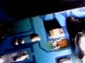
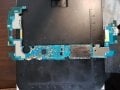
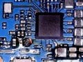
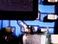
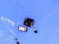
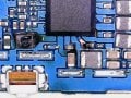
Hi guys! I am not a very big professionnal, still, I am trying to do something as I very much like the elctronics. I even have some studies in this field, but it was very long time ago, about 20 years. I have some components (SMD) that just burned out. I cannot identify them. I would need some help with this... Please let me know if someone can help me with this. Tnx.
 

Attachments

MrChips

Joined Oct 2, 2009
30,706
Welcome to AAC!

There is little hope in trying to identify a burnt out black component with no visible markings.
For starters, tell us the make and model of the unit.
Next, besides a close up as you have provided, show us the big picture so the we can see the whole board or sections of the board if it is a very large board.
 

pmd34

Joined Feb 22, 2014
527
The main one looks like a small SMD inductor. They come in many values however so your best bet would be to try and identifiy the IC that it is connected to. When things burn, they usually take other components with them however, so it would be questionable as to whether or not the IC itself still functions properly.
 

Thread Starter

Greg0405

Joined Jan 13, 2020
6
Tnx. I also think the IC is dead, since it is due to a water damage. It is a logic board of a smartphone: LG X Power 3. Water first got to the capacitors (see the image). There was a shield on all circuits and water just eneterd under as there is a quite big hole under the shield. I also suppose it to be an inductor as I can see some coils in it. It is the power supply for sound module on the logic board of the phone. As you can see from image, water (being more specific sea water) entered in the whole under the shield (see the arrow) and first of all reached/shorted the capacitor. Next, (luckily) it destroyed the IC and the IC destroyed the inductor... Or something like that. It is not a big deal to replace the IC, the question is what are the components that I identified visually that have to be replaced. As soon as I manage to make a picture of the entire board you will see that even lands and some traces were so much heated that those are detached from the board... I have no idea if there is a hope for such a board, but I will try, with your help maybe to do something, at least I will learn and acquire some new skills by soldering and desoldering micro components. By the way, for the others, do you think those 2 other components are capacitors? (see the picture bolow)
Thank you in advance.Sun Jan 12 16-08-25.jpg
 

Thread Starter

Greg0405

Joined Jan 13, 2020
6
Well... It is early to say that, I would give it a chance :) I still have some hope :D I will change the chip and the elements, and see what will happen. If I manage to resuscitate it, I will give you my feedback :)
 

Thread Starter

Greg0405

Joined Jan 13, 2020
6
What makes me skeptic is that I do not have ani schematics and I have no idea what components are also dead around this IC... I mean I will change it but I am a bit concerned about burn it out again due to the other components that caused its death... Before changing it I must be sure that other components are ok... Which is not so easy, taking into consideration that the inductor, for instance is not recognizable...there are also some capacitors, their values I can identify by their size... As for the inductor...
 

pmd34

Joined Feb 22, 2014
527
Hmm.. you cant go on the size of the capacitors to get their value as most sizes come in most values! But it looks like it is part of a switching regulator, so the biggest ones are likely to be not so critical in value.
For fixing things though I would be more worried as to what caused the inductor to burn up in the first place, something somewhere else must have tried to take to much power. And its a little strange to see this kind of "mess" on an SMD capacitor. The smallest component you have ringed actually looks grey in colour which could be a small inductor, as capacitors are usually the same orangy red colour. It could be a high frequency blocking inductor, that has had too much power across it as it looks like it has melted the solder mask on one end of the PCB..
All in all im sort of inclined to go with @MrChips on this, but I dont think if it was my stuff I would give up easily also!
I would however be tempted to have a poke about with a scope on the IC, and see if it has any signs of life, any pulses on any pins. If not then you can be more sure that fixing the components wont help.
 

MrChips

Joined Oct 2, 2009
30,706
BTW, if ever you are so unfortunate to have water into electronics, good advice says to make sure that the unit is completely dried out before applying power.

The first step would be to remove any power source, i.e. the battery.
Even after trying to remove any visible signs of moisture by whatever means, you should allow the unit to sit in a desiccator for at least 5-10 days. A homemade recipe is to enclose the unit with uncooked rice in a sealed plastic bag for 10 days.

Keep this tip in mind if it should ever happen to you.
 

Thread Starter

Greg0405

Joined Jan 13, 2020
6
Thx. By the way, this is not my phone, but this is another story. I just got permission from the owner to try to resuscitate it, even if I do not feel too confident to manage to do it. but...

As a matter of fact, the phone works perfectly, but only with BT garniture. No sound... no ring, no nothing.

So, here I am back. I managed to take some pictures of the board. See those attached. I also took some pictures to show how water reached and what elements it reached first.

So look at the pictures. I know, I know, the paths are a bit horrible, I still would like to see what can I do with it. The most important question I cannot answer is: what kind of inductor is this? I also would like you to tell me: there are some components that are one side connected to something, and another one has not path... I mean a component connected only on one side. (see picture 1). I also attach the picture of the entire logic board. So, as you can see, the water entered in many places (see the blue arrows). And I think it`s not a surprise to burn exactly the components that are close to the places where water infiltrated. See the places of components that I removed (red arrows). Unfortunately, even the paths of the components suffered not only because of my soldering skills but also due to the overheat caused by a short circuit. So, after cleaning everything around with isopropyl, I thought it might work... I connected the battery... and the inductor just burned like a torch The phone works as it worked before. There is a kind of noise in the headphones. I presume that there is still a short circuit somewhere, most probably in the IC and I will be glad to replace it, but!!! I have no idea what is the parameter of this inductor... what kind of SMD components are the others... are those capacitors? Are those also some inductors? I mean I understand that it is not a piece of cake to deal with it, and that's why I look for some help. I will also attach other images, in case those might be useful.

Tnx in advance. I am not obsessed with this phone, but maybe, if I might fix this issue, this case might be interesting and useful for others ;)
 

Attachments

Last edited:
Top