That's because of arbitrary-rules,
not because there aren't a ton of very experienced engineers here who only
took-up the challenge to relieve their boredom.
Try asking something like,
"how would You demonstrate, and create interest in, an easy to build project
that has a valuable purpose, and is easy to visually understand" ?
Sorry, my sentence was meant to say ‘now found a solution’ instead of ‘not found a solution’.
These experienced engineers have contributed to a practical solution to a practical problem. What’s to complain about? That’s what engineers do . . .
Having two clock periods ("timer intervals") probably is the more simple solution, but the circuit in #104 has a possible issue. During the operation of SW2, there is point when neither pot is connected. As long as the oscillator does not jump up to a megahertz frequency, this is not a huge problem because whatever this does to the clock timing is divided by at least 4096. But a better way to go is to have the normal-mode pot connected permanently to R15, and the set-mode pot switched in parallel with it. Now, the switch requirement is SPST, not SPDT, and it can be any simple, bouncy pushbutton switch.
I will have to look up the POR circuit in order to add that in but it seems to be a useful addition. There seem to be quite a few designs options.
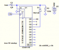
I can make my first timer interval even shorter than the approx 15s at the moment by choosing a smaller value of C1 for the oscillator. Around 5s would be good but the tolerance of these small ceramic caps can be rubbish so I need to measure them first to select an appropriate one.
I’m working on the PCB design now and have decided to add two LEDs for each pair of relays/device, one to indicate it is ‘operating’ and delivering power and another to indicate ‘charging’ and is receiving power. That would also be handy to indicate the overall state of the system.
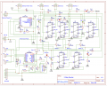
Later today I will post the revised schematic with the ‘POR’ so please can you confirm that it’s right. Thank you
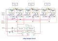
I have adapted the 'layout' graphic to show the inclusion of the indicator LEDs for 'operating' and 'charging'. This was a bit more involved than hoped for as blocking diodes are required at various places so that when one device is operating, its voltage does not turn on LEDs in the other operating branches. Similarly with the 'charging' LEDs. I can't see a way around this so a little 'wasted' voltage across the diodes. The result is here:
Regarding the schematic, this has been updated and also includes Crutschow's POR as suggested by AnalogKid.
Yikes! Well, I will have to go with the one I'm in the middle of, after doing all the follow-through, but if it doesn't work or is problematic, then I will give this a try.
Can you elaborate on the 3-shot monoshot (monostable?) timer? Is that 3 x a '555', with associated circuitry, and with pin 3 from each of them being the '1,2 &3' in your diagram? If so then I expect that each of the 555s can share the RC networks for simultaneous function.
Good show.
That looks to be the simplest solution.
So does your monoshot sequence timer have a delay between states to avoid overlap?
That could be done with a RC-diode actuate (but not release) delay to each relay driver (not shown in your schematic).
I have adapted the 'layout' graphic to show the inclusion of the indicator LEDs for 'operating' and 'charging'. This was a bit more involved than hoped for as blocking diodes are required at various places so that when one device is operating, its voltage does not turn on LEDs in the other operating branches. Similarly with the 'charging' LEDs. I can't see a way around this so a little 'wasted' voltage across the diodes.
1. The symbol you are using is for a zener diode, not a simple rectifier.
2. It looks like you have the full I/O current running through the added diodes. A 1N4148 cannot handle 10 A. How badly do you want those LEDs? 20 A Schottky diodes will need heatsinks, an increase in size, heat, and cost.
That can be the same 4060 / 4017 circuit you have now. He is describing it as three monostables, but deriving the coil signals from a counter is a better way to minimize overlap.
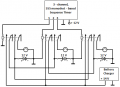
The circuit shows one common battery charger, but three separate loads. Up till now, the requirement has been to switch three batteries to one common load, the "Operate" output.
1. The symbol you are using is for a zener diode, not a simple rectifier.
2. It looks like you have the full I/O current running through the added diodes. A 1N4148 cannot handle 10 A. How badly do you want those LEDs? 20 A Schottky diodes will need heatsinks, an increase in size, heat, and cost.
I pulled the diode out of a library so they must have it wrong in there.
In the layout diagram I haven’t included the 10k resistors but in the schematic they are there between the diode and ground, so I’m not putting the full current through them. They are on ‘branch lines’. Shouldn’t that be fine?
The circuit shows one common battery charger, but three separate loads. Up till now, the requirement has been to switch three batteries to one common load, the "Operate" output.
Good show.
That looks to be the simplest solution.
So does your monoshot sequence timer have a delay between states to avoid overlap?
That could be done with a RC-diode actuate (but not release) delay to each relay driver (not shown in your schematic).
The circuit shows one common battery charger, but three separate loads. Up till now, the requirement has been to switch three batteries to one common load, the "Operate" output.
ak
The circuit shows one common battery charger, but three separate loads. Up till now, the requirement has been to switch three batteries to one common load, the "Operate" output.
No, device 1,2&3 are separate devices (batteries in this case) and they each in turn drive the same load. Equally they are charged in turn by the same charger. The load and charger are not shown on the schematic except as ‘Device Power Out’ and ‘In’
So you are not considering changing to Nandu's circuit which halves the number of relays and reduces the amount of wiring?
It adheres to the KISS principle, which I try to follow.
Edit:
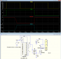
Below is a delay-on, no-delay-off, driver circuit that could be used to drive the three relays to prevent overlap:
All this to avoid using a microcontroller. 14 pin PIC, capacitor, 6 SPDT relays, 6 MOSFETs, 6 flyback diodes, and you are done. A switch to advance manually if you still want that. Can update, change the timing, change the sequence at will via programming. If an engineer working for me proposed what is proposed here, they would be fired.

 Facebook
 Google
 GitHub
 Linkedin