A better way to access STM32 registers

Thread Starter

ApacheKid

Joined Jan 12, 2015
1,762
This is quite surprising, a simple demo project using LL library for blinking LEDs, has this line of code:

Code:
    LL_GPIO_SetPinMode(GPIOD, LL_GPIO_PIN_12, LL_GPIO_MODE_OUTPUT);
That's readable I suppose and I traced through the definitions and found there are various macros that do bit shifting and so on. But when examining the generated code, I was surprised to see an ARM branch and link br instruction to some address, I went to that address and see a huge block of code generated from those bitshifts.

Building in release mode seems to more or less generate the same chunk of code but it does inline it and condense it:

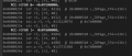
Using a bitfield typedef generates this:

1707433838379.png

The code generated for the LL function is:
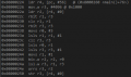
1707434147529.png

This seems to show that this technique of using lots of nested macros to manipulate and set register bits, does carry some overhead.
 
Last edited:

Thread Starter

ApacheKid

Joined Jan 12, 2015
1,762
I'm studying example code (that works) to understand exactly how registers are being set on an STM32F407VG.

Here is the code (from a well known book)

C:
    RCC->AHB1ENR |= 1;
    RCC->CFGR &= ~0x07E00000;
    RCC->CFGR |=  0x07600000;
   
    GPIOA->MODER |= 0x00020000;
    GPIOA->AFR[1] &= ~3; // F ?
    GPIOA->OSPEEDR |= 3 << 8 * 2;
   
    // Set HSE on
    RCC->CR &= ~0x000F0000;
    RCC->CR |=  0x00010000;
   
    while (!(RCC->CR & 0x00020000)) ;
   
    RCC->CFGR &=  ~0x00000003;
    RCC->PLLCFGR = 0x00402D04;
    RCC->CR |=     0x01000000;
   
    while (!(RCC->CR & 0x02000000)) ;
   
    FLASH->ACR = 0x0705;
   
    RCC->CFGR &= ~0x000000F0;
    RCC->CFGR |=  0x00000002;
   
    while ((RCC->CFGR & 0x0C) != 0x08) ;
The code is setting the device to use the HSE clock and to also drive PA8 at clock / 5, driving PA8 from the clock is a supported hardware feature.
The code works, I can see the 36MHx signal on PA8.

But unravelling exactly what it is doing to the registers is challenging, something I find puzzling is the convention of this:

Code:
    RCC->CFGR &= ~0x07E00000;
Surely this is the same as this if written out in full:

Code:
    RCC->CFGR = RCC->CFGR & 0xF81FFFF;
(I don't care about the &= I just wrote that out so its crystal clear) why do they not write the Hex as I did, why the need to use ~ ?
 
Last edited by a moderator:

MrChips

Joined Oct 2, 2009
34,954
Bit masking operations

Let us look at a simple example on how to use boolean OR and boolean AND operators.
Suppose you have a 4-bit register with unknown state XXXX.

Suppose we want to alter bit-0 without changing all other bits.
We create a bit-mask 0001 which specifies that we are interested in bit-0 only.

To set bit-0 to 1, we use the boolean OR operator:
XXXX OR 0001 => XXX1

To clear bit-0 to 0, we use the boolean AND operator with a different bit-mask. The bit-mask we need is 1110.
Hence,
XXXX AND (NOT 0001) => XXX0

Hope this makes it clear.
 

nsaspook

Joined Aug 27, 2009
16,363
It's done to confuse programmers that don't really understand hardware logic design. :D

https://eng.libretexts.org/Bookshel...5:_Setting_Clearing_and_Reading_Register_Bits

Clearing bits requires ANDing with a bitmask that has been complemented. In other words, all 1s and 0s have been reversed in the bit pattern. If, for example, we want to clear the 0th and 4th bits, we’d first complement the bit pattern 0x11 yielding 0xee. Then we AND:

1DDR &= 0xee;
Often, it’s easier to just use the logical complement operator on the original bit pattern and then AND it:

1DDR &= (~0x11);
 

Thread Starter

ApacheKid

Joined Jan 12, 2015
1,762
Bit masking operations

Let us look at a simple example on how to use boolean OR and boolean AND operators.
Suppose you have a 4-bit register with unknown state XXXX.

Suppose we want to alter bit-0 without changing all other bits.
We create a bit-mask 0001 which specifies that we are interested in bit-0 only.

To set bit-0 to 1, we use the boolean OR operator:
XXXX OR 0001 => XXX1

To clear bit-0 to 0, we use the boolean AND operator with a different bit-mask. The bit-mask we need is 1110.
Hence,
XXXX AND (NOT 0001) => XXX0

Hope this makes it clear.
Yes I see now. Although I'm perfectly at home with boolean algebra and have used it for decades, the use of the ~ was confusing me, trying to see exactly what register fields are being set or cleared or adjusted is extremely slow going.

This (after unravelling)
C:
RCC->CFGR &=  ~0x00000003;
RCC->PLLCFGR = 0x00402D04;
RCC->CR |=     0x01000000;
Is actually this
C:
    ahb1_ptr->RCC.CFGR.SW = 0;
    ahb1_ptr->RCC.PLLCFGR.PLL_M = 4;
    ahb1_ptr->RCC.PLLCFGR.PLL_N = 180;
    ahb1_ptr->RCC.PLLCFGR.PLL_SRC = 1;
    ahb1_ptr->RCC.CR.PLL_ON = 1;
 

MrChips

Joined Oct 2, 2009
34,954
By the way, this has nothing to do with STM32 or with the C programming language. This is basic boolean algebra.

And by the way, values such as 0x00402D04 are called literal constants. We don't use literal constants because they are likely to break.
 

Thread Starter

ApacheKid

Joined Jan 12, 2015
1,762
By the way, this has nothing to do with STM32 or with the C programming language. This is basic boolean algebra.
Thank you for the condescension.

My question was specifically about the practice of using the ~ in front of the literal constant, it was not about boolean algebra which is a discipline I learned fifty years ago. My question was not asking what it means, but why do they use the ones complement.
 

nsaspook

Joined Aug 27, 2009
16,363
...
My question was specifically about the practice of using the ~ in front of the literal constant, it was not about boolean algebra which is a discipline I learned fifty years ago. My question was not asking what it means, but why do they use the ones complement.
It's used to keep a consistent pattern (a bit high is a possible modification of set or clear) of bit manipulation constants in software that are compatible with a chip level, 'high' true, logic bit (in usually atomic instructions on registers) manipulations for set/clear operations. It makes the software easier to follow if literal constants are being used.
 

MrChips

Joined Oct 2, 2009
34,954
As I understand it, the ~ operator in C is a unary operator which forms the 1's complement of its argument.
This avoids having to create two different bit-masks when setting and clearing bits in a word.
 

Papabravo

Joined Feb 24, 2006
22,084
For the &= and & operators with a complemented mask the operations are clear & preserve. The 1's in the mask show you the field(s) to clear. The remaining bits are preserved.

For the |= and | operators with an uncomplemented mask the operations are set and preserve. The 1's in the mask show you the fields to set. The remaining bits are preserved.

The original reason for the existence of assignment operators was to allow the compiler to generate more efficient code in the case where the code did not have to fetch two distinct operands and store the result in a third. The first C compiler ran on an incredibly primitive machine (ca. 1978). You could probably make a rational argument that they are no longer needed, but some programmers have become accustomed to them so I would expect at least some resistance from them.

ETA: If I recall correctly an assignment operator could be performed with two instructions. The first loaded the constant mask, and the second instruction was a Read-Modify-Write Instruction, that read the memory location, did the logical operation, and wrote the result back to memory.
 
Last edited:

nsaspook

Joined Aug 27, 2009
16,363
For the &= and & operators with a complemented mask the operations are clear & preserve. The 1's in the mask show you the field(s) to clear. The remaining bits are preserved.

For the |= and | operators with an uncomplemented mask the operations are set and preserve. The 1's in the mask show you the fields to set. The remaining bits are preserved.

The original reason for the existence of assignment operators was to allow the compiler to generate more efficient code in the case where the code did not have to fetch two distinct operands and store the result in a third. The first C compiler ran on an incredibly primitive machine (ca. 1978). You could probably make a rational argument that they are no longer needed, but some programmers have become accustomed to them so I would expect at least some resistance from them.

ETA: If I recall correctly an assignment operator could be performed with two instructions. The first loaded the constant mask, and the second instruction was a Read-Modify-Write Instruction, that read the memory location, did the logical operation, and wrote the result back to memory.
Yes, the Read-Modify-Write Instruction being 'atomic' for the entire register simplified mutex locking (to prevent races and variable memory corruption) requirements for interrupt and thread based processing.
 

Thread Starter

ApacheKid

Joined Jan 12, 2015
1,762
Yes, the Read-Modify-Write Instruction being 'atomic' for the entire register simplified mutex locking (to prevent races and variable memory corruption) requirements for interrupt and thread based processing.
I don't see this on Arm though, what I mean is that looking at the assembler code (albeit not an instruction set I'm an expert on) there seems to be no read-modify write at all:

Look:

1707748335374.png

An interrupt could occur right before the str on 0x0800023E and the handler could write whatever value it wants, which would be wiped out by the eventual str after the handler completes and execution resumes.

Furthermore the update to the register occurs in two phases with no atomicity:

1707748666840.png

An interrupt could happen between the &= and the |= too.

If this was the GPIO ODR register where different code was manipulating different (independent) port pins then the above code is a recipe for disaster surely?

I see no r-m-w going on with these peripheral register at all, perhaps I'm misunderstanding what you guys are referring to here but as I see it the code needs additional explicit r-m-w protection not mentioned in the books I am using.

In OS work I've done in the past such code is often wrapped within a spin lock (basically an atomic test and set operation). These are used heavily for example in the Windows driver model.
 
Last edited:

Papabravo

Joined Feb 24, 2006
22,084
I don't see this on Arm though, what I mean is that looking at the assembler code (albeit not an instruction set I'm an expert on) there seems to be no read-modify write at all:

Look:

View attachment 315054

An interrupt could occur right before the str on 0x0800023E and the handler could write whatever value it wants, which would be wiped out by the eventual str after the handler completes and execution resumes.

Furthermore the update to the register occurs in two phases with no atomicity:

View attachment 315057

An interrupt could happen between the &= and the |= too.

If this was the GPIO ODR register where different code was manipulating different (independent) port pins then the above code is a recipe for disaster surely?

I see no r-m-w going on with these peripheral register at all, perhaps I'm misunderstanding what you guys are referring to here but as I see it the code needs additional explicit r-m-w protection not mentioned in the books I am using.

In OS work I've done in the past such code is often wrapped within a spin lock (basically an atomic test and set operation). These are used heavily for example in the Windows driver model.
That is because on a RISC (Reduced Instruction Set Computer) machine, of which the ARM is an example, ALL arithmetic and logical operations are done on REGISTERS. The ARM architecture is an example of a 3-address machine. The instructions have an immediate constant, a source register and a destination register. The Read-Modify-Write instructions are appropriate to a single address architecture with an implied register. This implied register is also known as an Accumulator.
 

Thread Starter

ApacheKid

Joined Jan 12, 2015
1,762
That is because on a RISC (Reduced Instruction Set Computer) machine, of which the ARM is an example, ALL arithmetic and logical operations are done on REGISTERS. The ARM architecture is an example of a 3-address machine. The instructions have an immediate constant, a source register and a destination register. The Read-Modify-Write instructions are appropriate to a single address architecture with an implied register. This implied register is also known as an Accumulator.
That's all well and good, but how does one implement a compare and swap? Well it seems this is one way using C on an ARM:

1707774655125.png

This is pretty standard and very similar to stuff I used in the past when working on shared/mapped memory on minicomputers, this is a true atomic read-modify-write.
 

Attachments

Papabravo

Joined Feb 24, 2006
22,084
That all well and good, but how does one implement a compare and sawp? Well it seems this is one way using C on an ARM:

View attachment 315100

This is pretty standard and very similar to stuff I used in the past when working on shared/mapped memory on minicomputers.
Yes, that seems to have the right flavor and also seems to be architecture independent. Still, it would be nice to see the details, which I can imagine, but not confirm. What is the reason for telling part of a story?
 

Thread Starter

ApacheKid

Joined Jan 12, 2015
1,762
I found a neat way to represent the various STM32 peripheral constants. By using a simple naming convention we can leverage this kind of macro:

Code:
#define MODER(X) MODER_ ## X

#define MODER_INPUT 0
#define MODER_GENERAL 1
#define MODER_ALTERNATE 2
#define MODER_ANALOG 3
Then refer to these in a slightly more helpful form:

Code:
ahb1_ptr->GPIO_D.MODER.MODER_12 = MODER(GENERAL);
Helps to overcome the C limitation that we can't #define constants within namespaces.
 
Last edited:

BobaMosfet

Joined Jul 1, 2009
2,211
I was playing with a simple demo that sets up the clock on an STM32F4 board, I got the demo working.

But I didn't like the look of the code, for example

C:
    RCC->CFGR &=   ~0x07E00000;
    RCC->CFGR |=    0x07600000;
If that's not clear to you, join the club. It's actually setting the MC01 clock output pin to be driven by the PLL and the MC01PRE (the divider) to 7 (divide by 5).

But by defining a simple bit field typedef and a macro, that code can be rewritten:

C:
    RCC_CFGR->MCO1 = 3;
    RCC_CFGR->MCO1_PRE = 7;
Not only is this much more readable, it leads to less generated machine instructions too:

View attachment 314599

all of a sudden this "low level" code started to look less low level.

Why on earth didn't ST do something like that, if they'd just defined a bitfield typedef for each of these various registers, and an associated simple macro, it would so much easier to follow examples and samples and so on. Furthermore, by making the typedef contain a union where the entire datum is just an int32, we can use that member to zeroize the entire register:

C:
    RCC_CFGR->ALLBITS = 0;
Here's the typedef and macro:

C:
#define RCC_CFGR ((CFGR_Type_ptr)&(RCC->CFGR))

typedef union
{
    struct
    {
        __IO BIT SW : 2;
        __IO BIT SWS : 2;
        __IO BIT HPRE : 4;
        __IO BIT UNUSED2 : 2;
        __IO BIT PPRE1 : 3;
        __IO BIT PPRE2 : 3;
        __IO BIT RTCPRE : 5;
        __IO BIT MCO1 : 2;
        __IO BIT UNUSED1 : 1;
        __IO BIT MCO1_PRE : 3;
        __IO BIT MCO2_PRE : 3;
        __IO BIT MCO2 : 2;
  
    };
    uint32_t ALLBITS;
} CFGR_Type, * CFGR_Type_ptr;
ST's job isn't to do what you did. It gives _you_ the complete control and freedom to use things your way. These are the ways in which superior developers do things other people are amazed at- by understanding and knowing not just the machine, but the compiler as well.
 

Thread Starter

ApacheKid

Joined Jan 12, 2015
1,762
ST's job isn't to do what you did. It gives _you_ the complete control and freedom to use things your way. These are the ways in which superior developers do things other people are amazed at- by understanding and knowing not just the machine, but the compiler as well.
As a non-professional microcontroller person, I have found it pretty challenging to get to grips with these devices, certainly when I first started. I could see they have a HAL API and an LL API, yet these are very large and quite daunting, not clear what API calls to use to do certain things. I did use them to get a decent interaction with an attached SPI device (an NRF24xxx).

But it was a struggle. Over the past week I stepped right back and started to look at the device and peripherals as-is, rather than through these APIs.

There's a uniformity there that's kind of hidden when using the API and so by defining bitfield structs that correspond to peripheral registers it started to look less daunting.

We have buses and buses have peripherals and peripherals have registers and registers have bitfields and that's it. The documentation for these peripherals and registers is very good and very detailed and I'm finding myself able to work with these more than I was able to with the HAL or LL.

I've removed, completely removed all of the STM header files, LL and HAL headers and reduced a little project to a small easy to understand minimal form.

Here's how a bus is defined in this scheme:


C:
typedef struct
{
    // There is padding between peripherals that forces
    // each one's start address to be at a particular offset
    // from the preceding peripherals start address.
    GPIO_Regset GPIO_A;
    PADTO(1024, GPIO_Regset,a);
    GPIO_Regset GPIO_B;
    PADTO(1024, GPIO_Regset,b);
    GPIO_Regset GPIO_C;
    PADTO(1024, GPIO_Regset,c);
    GPIO_Regset GPIO_D;
    PADTO(1024, GPIO_Regset,d);
    GPIO_Regset GPIO_E;
    PADTO(1024, GPIO_Regset,e);
    GPIO_Regset GPIO_F;
    PADTO(1024, GPIO_Regset,f);
    GPIO_Regset GPIO_G;
    PADTO(1024, GPIO_Regset,g);
    GPIO_Regset GPIO_H;
    PADTO(1024, GPIO_Regset,h);
    GPIO_Regset GPIO_I;
    PADTO(1024, GPIO_Regset,i);
    GPIO_Regset GPIO_J;
    PADTO(1024, GPIO_Regset,j);
    GPIO_Regset GPIO_K;
    PADTO(2048, GPIO_Regset,k);
    CRC_Regset CRC;
    PADTO(2048, CRC_Regset,l);
    RCC_Regset RCC;
    PADTO(1024, RCC_Regset,m);
    FLASH_Regset FLASH;

} AHB1_Bus, *AHB1_Bus_ptr;
The PADTO macro enables me to position the following member at a defined offset from the start of the preceding member and so far is working fine, code runs and behaves as expected.
 
Last edited:

MrChips

Joined Oct 2, 2009
34,954
I have stated this once before. This has nothing to do with STM32 MCUs. This applies across the board with all MCUs.
Some MCUs and their peripherals are more complex than others.

We don't use bit fields at the raw binary bit level. We use the defined labels supplied in the device header file.
Thus when bit assignments change from one device to another, the code will not break.
 

Thread Starter

ApacheKid

Joined Jan 12, 2015
1,762
I have stated this once before. This has nothing to do with STM32 MCUs. This applies across the board with all MCUs.
Some MCUs and their peripherals are more complex than others.

We don't use bit fields at the raw binary bit level. We use the defined labels supplied in the device header file.
Thus when bit assignments change from one device to another, the code will not break.
I understand the conventions and practices used by professional engineers and the various pros and cons involved.

As for code breaking that is no more a risk for bitfields than it is for predefined offsets, one simply uses a typedefs header appropriate for the device, that is just as the explicit offset constants are defined per-device, so too can bitfields.

Clearly the typedefs I've defined so far pertain to STM32F407, for a different device I'd like define a slightly different set.

I'm doing this for personal edification and to gain a better understanding of the MCUs, this isn't my job, I don't have any customers.
 
Top