6W (i guess) mini bass guitar amplifier design issues

Thread Starter

Snortuff

Joined Dec 20, 2023
6
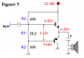
Is that a speaker eliminator? Speakers do not like DC. That circuit will eliminate your speakers in no time. Make a note of where you found it and don’t look there for circuits in the future.

The volume control potentiometer goes between the output of the last stage of the preamp and the input of the power amp.
The circuit diagram you posted in post #17 is rather unconventional, besides being totally useless.
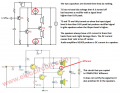
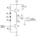
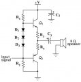
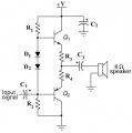
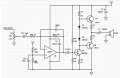
Thanks for your answers. I might choose the wrong power input symbol. In the attachments I shared the circuit mono-amplifier-two-speaker that I found on a website where you might see the watermark. Is the circuit totally useless or did I make a mistake?

Sorry I am a slow learner and just wanted to learn about the very basics of audio electronics and I thought the need of a practice amp might be a starting point for me. thank you very much for your patience


When I have some time today I will introduce you to the basics of transistor amplifier design.

Thank you again. I would like to not take your personal time but if you can suggest a resource that i can read i appreciate it.
 

Thread Starter

Snortuff

Joined Dec 20, 2023
6
The amplifier circuit in post #17 is horrible. The power output stage has many errors. Schematic is edited.
Oh, I messed up when I tried to redraw the original circuit. Thank you for pointing this out. I will try to correct the Schematic as it should be as in the original.
 

Audioguru again

Joined Oct 21, 2019
6,826
If you ignor the sounds produced by the DC current slamming the speaker coils into their magnet structures, then each 4 ohms speaker gets a maximum of 8V peak-to-peak (a little less than the 9V supply) and an average current of 4V/4 ohms= 1A. The output power from each speaker is only 2W. The transistor between the speakers and each speaker heat with 2.67V x 0.67A= 1.8W all the time (even when not playing sounds).
 

MisterBill2

Joined Jan 23, 2018
27,979
The circuit diagram you posted in post #17 is rather unconventional, besides being totally useless.

When I have some time today I will introduce you to the basics of transistor amplifier design.
To be more specific than MRchips, no part of the circuit will work as desired. I presented a source of useful information.
No portion of this circuit is able to work. Trace the signal path to understand what I mean.

Once again I suggest a source of working circuits to copy.
 

MrChips

Joined Oct 2, 2009
35,017
Transistors
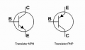
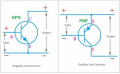
Let us begin with the two types of BJTs (Bipolar Junction Transistor), PNP and NPN.

1703268461957.png

The two transistors are functionally the same. What is different is the polarity of the voltages required to make the circuit function. It is useful to know when and where you use the one and not the other.

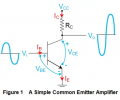
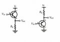
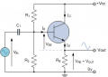
Common Emitter Amplifier

1703268831753.png


In a common emitter amplifier configuration, the output signal is taken from the collector. This configuration can provide voltage gain and the output signal is inverted, i.e. voltage gain is negative.

1703269401483.png


Common Collector Amplifier

A common collector amplifier provides current gain (low output impedance) and less than unity voltage gain. The output signal is in phase with the input. It also inherently provides negative feedback. As the emitter current rises, the voltage across the emitter resistor also rises thus reducing the base-emitter bias voltage. This provides a negative controlling effect that reduces distortion and also reduces temperature instability.
common collector NPN PNP.jpg

1703271877171.png

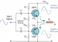
Common Collector Push-pull Amplifier

For an audio power output amplifier, we want high current output, i.e. low output impedance. For that, we choose common collector configuration. The upper transistor (NPN) supplies current on the positive half of the waveform while the lower transistor (PNP) sinks current on the lower half of the waveform.

If both transistors are conducting at the same time they both get hot and waste current. This is Class A operation. If only one transistor is conducting then all the current goes to the load. This is more efficient and the transistors run cooler. This is Class B operation. It suffers from cross-over distortion when one transistor takes over from the other.

We can create a compromise by having the off-transistor conduct a little current. This reduces cross-over distortion and you guessed it, it is called Class AB operation. We can achieve this my adjusting the bias voltages on the base of the two transistors.

Note the symmetry of the circuit. In theory, the output signal to the load RL is symmetrical about the mid-point of the supply rails.

1703269199735.png


1703269659289.png


With single supply voltage, a DC blocking capacitor is needed to avoid having continuous current flowing through the loudspeaker.
 

MrChips

Joined Oct 2, 2009
35,017
I forgot to begin with an opening remark that you will be very disappointed with the performance of a simple transistor power amplifier as a mini bass guitar amplifier. Nevertheless, you should gain something from this brief power amplifier tutorial.

Power Calculation

As mentioned in a previous post, it is instructional to do a quick battery and power estimate.

Let us assume that the power source is a commonly available 12V SLAB (Sealed Lead Acid Battery) with no DC boost converter. SLABs are known to be reliable and robust given appropriate battery management.

Let us also assume that the nominal impedance of the loudspeaker is 8Ω which is the most common value.

12VDC peak-to-peak voltage is 6V amplitude, which is 6V / 1.4 = 4.3V rms (root mean square)
The maximum power delivered to an 8Ω load is,
P = V x V / R = 4.3 x 4.3 / 8 = 2.3W

The maximum power delivered to a 4Ω load is,
P = V x V / R = 4.3 x 4.3 / 4 = 4.6W


Power Amplifier Design

Based on the introductory discussion, we can create a preliminary design of the power amplifier stage.

Push-pull amplifier.jpg

Source supply voltage +V is +12VDC.

We want to select two power transistors with closely matched characteristics.
Q1 (NPN) TIP31 and Q2 (PNP) TIP32 is a popular complementary pair.

R3 and R4 are emitter resistors which will limit our short-circuit current and provide some degree of negative feedback.
Since the speaker impedance is 8Ω, we want R3 and R4 values to be below that. Making R3 and R4 each equal to 1Ω is a good starting point.

C3 is the DC blocking capacitor driving the 8Ω loudspeaker. The two constitute a high-pass filter and we have to make sure that we do not attenuate the lowest bass note, which is open E string at 41Hz. Go to an on-line high-pass filter calculator and determine the capacitance that gives a roll-off frequency of 20Hz. The calculated capacitance is just under 1000μF.
We will select C3 to be 1000μ/16V aluminum electrolytic capacitor. Pay attention to the polarity when you wire the circuit. The negative lead of the capacitor goes to the loudspeaker. We should also place a second 1000μ/16V aluminum electrolytic capacitor C2 across the power rails from +V to GND to smooth out the supply voltage.

Our next step is to set up the proper bias voltage on the base of the two transistors.
 

JohnSan

Joined Sep 15, 2018
130
Hello everyone, I am new to the circuit world. Now i am trying to design a mini bass guitar amplifier with my almost no knowledge

I have lots of basic components, especially the JRC4558, I know its not so good for audio but I have a lot of them so I wanted to use them.
For speakers I have 2 cheap speaker exciters (3W 4 ohm each) which I am planning to use both in the same panel.
Last but not least, if the circuit can work with a 9 volt battery it would be perfect.

I draw a simple circuit but now I can not calculate the component values for driving the exciters. I don't know how to calculate the output wattage.
I could not find a dual opamp in LTspice so I drew 2 op amps in series. Can this circuit work? and how can i calculate the component values for the exact output that i need?
Hi Snortstuff.

To 'design' any electronics circuits, you really need to start with some formal training in the associated discipline.
Eg. RF, Audio, Digital, Power, Robotics etc.

Typical courses are a degree in some form of electrical engineering, specialising in power, computing, robotics etc.

With the knowledge gained, you would never ask anything similar to your original question....
'Have lots of JRC4558 to make a 6W Bass amplifier'.

Your best bet at the moment is to use a circuit already proven or buy an amp.

(I'm amazed at some of the 'helpful' replies....).
J.
 

MisterBill2

Joined Jan 23, 2018
27,979
Hi Snortstuff.

To 'design' any electronics circuits, you really need to start with some formal training in the associated discipline.
Eg. RF, Audio, Digital, Power, Robotics etc.

Typical courses are a degree in some form of electrical engineering, specialising in power, computing, robotics etc.

With the knowledge gained, you would never ask anything similar to your original question....
'Have lots of JRC4558 to make a 6W Bass amplifier'.

Your best bet at the moment is to use a circuit already proven or buy an amp.

(I'm amazed at some of the 'helpful' replies....).
J.
Before you get to all of those things, basic circuit theory is very useful. Then an understanding of op-amps, at least the gain math and about reading the data sheets to understand the ratings.
I found a circuit for an 8 watt amplifier and also for a one watt headphone guitar amplifier. I will send them later.
 

MrChips

Joined Oct 2, 2009
35,017
Before we set the bias voltage on the base of the transistor, let us talk a bit about how a transistor behaves as an amplifier.

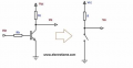
We often use a transistor as a switch that is either ON (closed) or OFF (open).

When the base voltage with respect to the emitter is zero, the switch is open. We say that the transistor is in cut-off mode.
When the base voltage is higher than 0.7V with respect to the emitter (for an NPN transistor), the switch is closed. We say that the transistor is in saturation mode.

1703298733418.png

Saturation mode and cut-off mode are two extreme conditions of the transistor.
What happens in between saturation and cut-off?
This is where the transistor becomes a linear amplifier with typical current gains from 50 to 300. In order to bias the base of the transistor in the linear mode we need to make the base-emitter voltage at least 0.65V or higher.

This is the purpose the diodes D1-D3 in the circuit diagram shown.

Push-pull amplifier.jpg

Diodes D1-D3 are typical small signal diodes such as 1N914 or 1N4148. The forward voltage of a PN junction is typically about 0.7 over a wide range of diode current. In other words, the diode acts as a 0.7V voltage stabilizer.

With three diodes in series, the voltage between the base of Q1 and the base of Q2 will be about 2V. This will bias the transistors in the linear region with very little cross-over distortion. However, Q1 and Q2 will run very hot (Class A mode).

(In any case, you need to mount Q1 and Q2 on separate heat sinks. Note that the tab on the TO-220 transistor is also the collector. Hence you don't want to short out the power supply.)

We can remove one of the diodes and run the transistors cooler. Now we have to tolerate some cross-over distortion. You can even replace the third diode with a variable resistor. Now you can trim the bias voltage to suit your taste while keeping the drain on the battery low. For now, we will just stay with two diodes for this part of the test.

How do we determine the value of resistors R1 and R2?
The maximum current through emitter resistor R3 is about 6V/9Ω which is about 600mA. Let's assume that the current gain of the transistor is about 100. We need to supply a base current of about 600mA/100 = 6mA.
The voltage across R1 is about 6V. This puts R1 at about 1kΩ. The same goes for R2.

Push-pull amplifier.jpg
Now that we have created the DC bias voltage on the base of Q1 and Q2, we want to protect it from any DC voltages at the input signal. Again, we use a DC blocking capacitor C1 of about 10μF/16V. This is called AC coupling. At a later stage, we will remove C1 when we create a DC coupled amplifier with negative feedback.

In the next post, we will discuss how to use an op-amp to drive the power output stage.
 

Audioguru again

Joined Oct 21, 2019
6,826
The schematic shows "+V" but no supply voltage. Previously it was +12V.
You want the emitter of the NPN output transistor to have a peak current of 600mA then the emitter voltage will be (600mA x 9 ohms=) 5.4V above the 6V idle voltage =11.4V.
BUT then the bias current in R1 will be ZERO mA and is impossible. Bootstrapping will help.

As the output current increases then the bias current decreases which is the opposite that you want. Then the resistance of R1 must be much less. Also, the minimum hFE of a TIP31 or TIP32 power transistor is only 5 at only 3A.
 
Last edited:

MrChips

Joined Oct 2, 2009
35,017
Welcome to the wonderful world of operational amplifiers (op amp or opamp for short). Besides the transistor, the op amp is the most significant device in the electronics designer's arsenal. The importance of the op amp lies in the fact that the circuit designer can utilize the device as a theoretical black box and can create complex functions with simple mathematical formulas. The designer need not be be concerned with the inner workings of the black box.

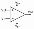
The basic op amp IC is a 5-terminal device.

1703348175500.png

There are two inputs, one output and two power supply pins, one positive and the other negative.
In many situations we can consider the real device to have theoretically ideal characteristics.

The ideal op amp has the following characteristics:
(1) Infinite input impedance. This means that the op amp can accept an input signal without altering that signal (by loading).
(2) Zero output impedanace. Since Ohm's Law states I = V / R, the op amp can supply an infinite amount of current from its output pin.
(3) Infinite voltage gain. The op amp can amplify the smallest voltage to an infinite voltage.
(4) Infinite bandwidth. The op amp can amplify all signals from zero frequency to infinite frequency.

That is the circuit designer's wish list. In reality, none of the above is possible. In practice, modern IC op amps can come very close to supporting most of the application's practical needs. This is where it is important to look at the datasheet of the device and examine how closely it meets those requirements.

Note (3) - In reality, the output voltage swing cannot exceed that of the power supply rails.

As an example, let us look at the datasheet of TL072 which is a popular JFET (junction field effect transistor) dual op amp in an 8-pin package.
Reference: https://www.ti.com/lit/ds/symlink/tl072.pdf

(1) Input impedance = 10MΩ
(2) Output impedance = 125Ω
(3) Open-loop voltage gain = 1000,000 = 120dB
(4) Gain-bandwidth product = 5MHz

Note (4) - Gain-bandwidth product gives both the voltage gain and maximum frequency limitations. At 5MHz, the voltage gain is reduced to 1.

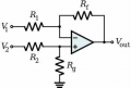
Basic Op Amp Circuit Configuration


1703350279908.png

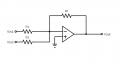
This is the basic differential op amp configuration. You want to memorize this circuit.
In general, R1 = R2 and Rf = Rg.

The voltage gain Av = -Rf /R1

Vout = Av (V1 - V2) = (-Rf/R1) x (V1 - V2)

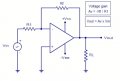
Inverting Amplifier

opamp inverting amplifier.jpg


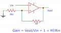
Non-inverting Amplifier


opamp non-inverting amplifier.jpg

Summing Amplifier
1703350956669.png

Points of note

(1) Op amps are not usually used with open-loop gain. Op amps with open-loop gain are sometimes used as analog comparator circuits.
(2) Op amps are generally configured with lots of negative feedback. When negative feedback is applied, the voltage at the inverting input will be the same as the voltage at the non-inverting input. (The very high open-loop gain of the op amp makes this happen.)
 

MrChips

Joined Oct 2, 2009
35,017
Dual Power Supply vs Single Power Supply

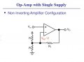
You may have noticed that the basic op amp circuits call for dual supply voltages also known as split supply. With balanced dual supply voltages, input and output signals are referenced with respect to 0V reference or COMMON.

If our goal is to use a single voltage supply, we need to create a reference voltage that is midway between the supply rails, i.e. at have the single supply voltage. The simplest way to implement this is with a voltage divider.

opamp single supply.jpg
Now that we have all the basics we need, we will apply this to an op amp configuration to drive the power amplifier stage.
I will use the popular LM358 dual op amp in an 8-pin DIP package. You can use the JRC4558 and it has the same pinout as the LM358.
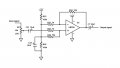
One op amp will be reserved to create a pre-amp for the guitar input.
opamp  single supply.jpg
The opamp is configured as a non-inverting amplifier with a moderate voltage gain of 10. R25 and R26 create a "pseudo-ground", in other words, a reference voltage at half the supply voltage. Both inverting and non-inverting inputs to the op amp are referenced to this reference voltage, filtered with C22.

We can apply some high frequency attenuation by inserting a capacitor across the feedback resistor R22.

The input signal is controlled by potentiometer VR1 which has a logarithmic taper. This will receive the guitar signal after being amplified by the preamp.

In the next post we will apply negative feedback and eliminate the AC coupling capacitor C1.
 

JohnSan

Joined Sep 15, 2018
130
Getting back to the original post.....

Project overview.
Requirement is:- Bass Amplifier, with 6 Watts power output, prefereably running off 9V battery supply.

Available resources:
Lots of basic components and JRC4558s.
Two cheap 3W 4 ohm speakers.
9V battery.
No knowledge.

Assessment.
JRC4558 minimum power supply spec is +/-5V.
So one 9V battery is not suitable without using a DC-DC converter.
Assumimg your stock of basic components does not contain such a device.
You will need two 9V batteries.

JRC4558 max O/P current is 25mA.
So can use all your stock of these to achieve a few watts output.

Based on 6W pk into 8 ohms.
Approx 7V, so 9V batteries are good.
I = 0.866, so 35 op amps required.


Bass guitar o/p up to 200mV.
Use a gain of approx 50 will achieve 6W pk, including some headroom.RC4558 amp.JPG

Bass guitar
F= 40 to 400Hz approx.

What is the frequency range of the available speakers?
Using two cheap 3W loudspeakers will likely define the final quality of the finished project.
It'll be absolute rubbish!

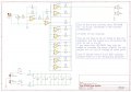
See the attached circuit.
It shows 5 x JRC4558's used.
One is used for pre-scaling the signal and includes a little filtering.
The other 4 show the classic Leader-Follower parallel amp configuration.
A further 13 of these need to be added, which should see your stock depleted somewhat.....

(I will add, this has not been tested, but please advise how you get on).
 

Audioguru again

Joined Oct 21, 2019
6,826
I agree that a cheap 3W speaker will sound awful. It will produce no bass sounds. A bass boost circuit does not boost anything, instead it simple reduces high frequencies, the bass will still be only a few Watts that the cheap little speakers will produce badly.
 

Ian0

Joined Aug 7, 2020
13,227
I agree that a cheap 3W speaker will sound awful. It will produce no bass sounds. A bass boost circuit does not boost anything, instead it simple reduces high frequencies, the bass will still be only a few Watts that the cheap little speakers will produce badly.
Yes. There's no substitute for cone area!
 

MrChips

Joined Oct 2, 2009
35,017
Update: I wanted to use a rail-to-rail single supply op amp but did not have any in stock. The design will be placed on hold until stock comes in. In the meantime, this is what I have.

On my final post, I would have made a note to the TS on the importance of cone size and more importantly the function of the speaker cabinet.

Edit: Corrections made to drawing.

AAC audio amplifier.jpg
 

JohnSan

Joined Sep 15, 2018
130
Update: I wanted to use a rail-to-rail single supply op amp but did not have any in stock. The design will be placed on hold until stock comes in. In the meantime, this is what have.

On my final post, I would have made a note to the TS on the importance of cone size and more importantly the function of the speaker cabinet.

View attachment 310816
In your previous post, you said would like to eliminate C1.
If you leave it connected like it is, it may eliminate itself.....
 

Audioguru again

Joined Oct 21, 2019
6,826
The power amplifier portion of the total amplifier produces 6V p-p output at clipping with an input of about 0.9V p-p. Therefore it does not need a rail-to-rail opamp as a preamp. Its voltage gain is about 6.67 times.
The output power at clipping is only 0.56W into 8 ohms. I do not have models of the TIP31 and TIP32 power transistors for my simulation that used more powerful transistors.
 
Top