 Facebook
 Google
 GitHub
 Linkedin
Hello Everyone,
I had recently studied a course on Computer Architecture. When studying about Memory, I came across SRAM and DRAM. Now, It just intrigued me to build a SRAM Cell because in one of the course I had studied about MOSFETs as well. I was successfully able to build a 6T SRAM Cell in Cadence where I wanted to simulate the graphs for all three modes of operation: 1.) Standby Mode, 2.) Read Mode , and 3.) Write Mode.
Till now, The Write Mode and Standby Mode work correctly but when it comes to Read Mode, I do not get the output waveforms that I need.
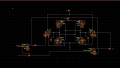
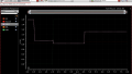
(I will attaching the photo of the Circuit and the Output waveform that I get for Read Mode). In Read Mode, I was expecting the Bit Line(BL to be at VDD) and the Bit Line Bar (BLB at 0) because those were the values that I wrote in the Write Mode. To check if the values were retained in the Write Mode, I also operated the circuit in the Standby Mode(where WL = 0) and the values were retained. However, The Circuit is not operating as I wanted in the Read Mode.
In this circuit, you can see that I have added two additional transistors, which connect VDD, Bit Lines (BL and BLB) and a Precharge Pin (I have made this pin, so that I can precharge the BL and BLB before the WL can be turned to HIGH, as that is one of the requirements for the Read Operation). So, in Read Mode, I try to pre-charge both Bit lines for about 1.5 microseconds because the WL turn high(VDD) at 2 microsecond onwards. Can you please assist with the Read Operation of this circuit please?
I had recently studied a course on Computer Architecture. When studying about Memory, I came across SRAM and DRAM. Now, It just intrigued me to build a SRAM Cell because in one of the course I had studied about MOSFETs as well. I was successfully able to build a 6T SRAM Cell in Cadence where I wanted to simulate the graphs for all three modes of operation: 1.) Standby Mode, 2.) Read Mode , and 3.) Write Mode.
Till now, The Write Mode and Standby Mode work correctly but when it comes to Read Mode, I do not get the output waveforms that I need.
(I will attaching the photo of the Circuit and the Output waveform that I get for Read Mode). In Read Mode, I was expecting the Bit Line(BL to be at VDD) and the Bit Line Bar (BLB at 0) because those were the values that I wrote in the Write Mode. To check if the values were retained in the Write Mode, I also operated the circuit in the Standby Mode(where WL = 0) and the values were retained. However, The Circuit is not operating as I wanted in the Read Mode.
In this circuit, you can see that I have added two additional transistors, which connect VDD, Bit Lines (BL and BLB) and a Precharge Pin (I have made this pin, so that I can precharge the BL and BLB before the WL can be turned to HIGH, as that is one of the requirements for the Read Operation). So, in Read Mode, I try to pre-charge both Bit lines for about 1.5 microseconds because the WL turn high(VDD) at 2 microsecond onwards. Can you please assist with the Read Operation of this circuit please?
Attachments
-
 546.7 KB Views: 13
 -
 713.8 KB Views: 13


