Facebook
 Google
 GitHub
 Linkedin
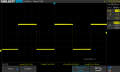
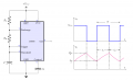
Hello,I’m designing a 555 timer circuit in astable mode to get ~50% duty cycle. I used two diodes to separate the charging and discharging paths, and used 100kΩ resistors on both paths (R2 = R1 = 100k). My reasoning was that since T_high = T_low, this should give ~50% duty cycle and when I tested it on the oscilloscope, it showed 49.5% / 50.5%, which was what I wanted.
My prof today looked at my design and said that I should have used a 101kΩ resistor in the Vcc side instead of the 1kΩ I used because resistors should be equal and its not right to use 1k for 50% duty cycle. I’m not sure why this matters in this design, since I thought with the diodes separating the paths, the timing should just depend on RA and RB now not the resistor connected to Vcc.
Also, My reasoning and calculation to justify my duty cycle is that
R1=charging path resistor
R2 = discharging path resistor
duty cylce =t_high/T_total = R1/(R1+R2)=100/(100+100)=50%
am I wrong for not considering R=1k at all in this formula ? my assumption was that R=1k it is just helping the capacitor charge fully, but it is not in the timing formula. and why should I use 101k for R ?
Would really appreciate if someone can clarify this.Thanks in advance
Last edited: