Facebook
 Google
 GitHub
 Linkedin
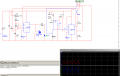
No, it sounds like you need a (latching?) circuit that activates after a complete clock cycle as opposed to one that activates on a high or low pulse. A D flip flop configured as a T flip flop mught work here, but I need to know more first.
I haven't read your entire post and it looks like there have been some changes, so let ask the following:
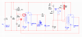
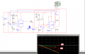
1) Is SW1 in your last schematic part of this two-switch activation or is it only to supply power to the circuit when it is being used? If the latter, I assume it is a toggle or rocker switch, correct?
2) Based on the last exchange between you and Bill, you want the following to occur?
a) User flips SW1 to apply power to circuit, but circuit does nothing yet.
b) User presses switch A and holds (nothing happens).
c) User presses switch B and holds (nothing happens).
d) User releases switch A and circuit begins.
3) Can user release switch B immediately after A is released or must they wait until circuit completes its mission, i.e., if user releases B before circuit finishes operation, the operation is stopped?
4) What is being turned on by the switch procedure? Only U2 or U1 & U2? My question being is U1 being used as part of the switch activation or is the switch activation used to turn on U1 (which later turns on U2)?
I haven't read your entire post and it looks like there have been some changes, so let ask the following:
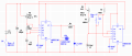
1) Is SW1 in your last schematic part of this two-switch activation or is it only to supply power to the circuit when it is being used? If the latter, I assume it is a toggle or rocker switch, correct?
2) Based on the last exchange between you and Bill, you want the following to occur?
a) User flips SW1 to apply power to circuit, but circuit does nothing yet.
b) User presses switch A and holds (nothing happens).
c) User presses switch B and holds (nothing happens).
d) User releases switch A and circuit begins.
3) Can user release switch B immediately after A is released or must they wait until circuit completes its mission, i.e., if user releases B before circuit finishes operation, the operation is stopped?
4) What is being turned on by the switch procedure? Only U2 or U1 & U2? My question being is U1 being used as part of the switch activation or is the switch activation used to turn on U1 (which later turns on U2)?