500mW amplifier design problem

Thread Starter

Pavle23

Joined Mar 14, 2022
2
Hi, I must design a 500mW (RMS) AB amplifier to drive an 8 ohm load. So I ended up with this:
1647241996531.png
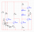
I used BCP54 and BCP51 as output transistors, Q3 to drive them both, Q4 for voltage gain, and Q5 for current gain which also adds a lot to input impedance. Input impedance has to be 50k ohm, and voltage gain of 100. I used BCPs current gain to be 60 and BC847Bs current gain to be 100. First thing I figured out is that Vpk of 8 Ohm load must be 2.8V, because: V=sqroot(500mW*8)*sqroot(2), and Ipk = 0.35A. So I decided that voltage swings on R3 resistor must be from 9V to 3.4V, and the Q3 Ic must be from 3.4mA to 9mA. Q3 is biased from Q4, and Q4 is biased from Q5. The problem is that my design doesn't work the way it should if I monitor voltage on the 8 ohm resistor with an oscilloscope.
1647241580941.png
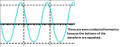
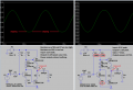
This is what I get if I use 50mV peak source 1kHz at the input. Sine wave is nice, but there is no enough voltage gain at all (I use A channel).
1647241776053.png
With 100mV and above peak1kHz, I get this. Again, not enough gain plus saturation. I tried to align it a little bit with the R5 potentiometer (according to the calculations, 100 ohm resistor should be there), but have no luck. So what have I done wrong? Any clues?
Thanks.
 

Attachments

Ramussons

Joined May 3, 2013
1,396
I find 2 major mistakes.
1) Disconnect the 8 Ohm load and do a bias voltage calculation on the transistors. The emitters of Q1 and Q2 must be about half the supply voltage, 6 volts. Are they?
2) With a single power supply, you will have to connect the 8 ohm load through a large DC blocking capacitor - at least 500 uF.
 

Thread Starter

Pavle23

Joined Mar 14, 2022
2
Do you mean I need to have 6V on bases of both transistors? Isn't it basically creating two A class amplifiers mixed together?
 

Ian0

Joined Aug 7, 2020
9,618
The main problem is it is running “open loop”. There is no DC feedback to stabilise the output voltage and no AC feedback to reduce the distortion - sell it to a guitarist!
 
Last edited:

Audioguru again

Joined Oct 21, 2019
6,647
You have a +12V supply and the output of the amplifier must swing up and down. Then the output of the emitter outputs must idle at +6.5V so that they can swing up a few volts and swing down a few volts.
Have you ever seen a speaker with 6.5V of DC on it? It might be smoking or it has its cone pulled over to one side and it buzzes a little with a signal. You must use a coupling capacitor that blocks the +6.5VDC but pass the AC to the speaker.

All audio amplifiers use DC and AC negative feedback from the output to near the input to stabilize the DC and reduce distortion that you have.

I simulated the output parts of your circuit but used different but similar transistors. transistors have a wide range of specs but your circuit has no DC negative feedback to reduce the range.
 

Attachments

Last edited:

Audioguru again

Joined Oct 21, 2019
6,647
I have a solid state stereo receiver that is 4 years newer than that 62 years old circuit also using a similar quasi-complementary circuit in its amplifier. A quasi-complementary was used because a good powerful PNP transistor was not made yet.
The patent mentions not using an output transformer like all tooob amplifiers used in those days.

When I bought the 58 years old receiver I sold my tooobs amplifier to an old geezer who did not know that transistors were invented.
 

Ian0

Joined Aug 7, 2020
9,618
I have a solid state stereo receiver that is 4 years newer than that 62 years old circuit also using a similar quasi-complementary circuit in its amplifier. A quasi-complementary was used because a good powerful PNP transistor was not made yet.
The patent mentions not using an output transformer like all tooob amplifiers used in those days.

When I bought the 58 years old receiver I sold my tooobs amplifier to an old geezer who did not know that transistors were invented.
With all due respect, a minor correction: in the days of germanium it’s the NPN that was lacking.
 

MrChips

Joined Oct 2, 2009
30,618
Do you mean I need to have 6V on bases of both transistors? Isn't it basically creating two A class amplifiers mixed together?
As already stated in post #2, R1 and R2 should be sitting at around 6V.
R8 is almost a short to GND.
Remove R8 and do the tests again.
 

Audioguru again

Joined Oct 21, 2019
6,647
I had a portable radio with germanium transistors about 64 years ago. I made little low power amplifiers with silicon transistors about 54 years ago and my high power amplifier used tooobs. My first stereo receiver had silicon output transistors (quasi-complementary with 2N3055 NPNs 57 years ago and it still works but its input selector switch is worn out.

The circuit posted in this thread uses complementary output transistors biased in class-AB. Its output transistors switch back and forth in class-B most of the time but the diodes bias them in low current class-A near idle to avoid class-B crossover distortion.
 

michael8

Joined Jan 11, 2015
408
I've rearranged your text order a bit and added some comments...

> First thing I figured out is that Vpk of 8 Ohm load must be 2.8V, because:
> V=sqroot(500mW*8)*sqroot(2), and Ipk = 0.35A.

That's a real good start.

> I used BCP54 and BCP51 as output transistors,

https://assets.nexperia.com/documents/data-sheet/BCP54_BCX54_BC54PA.pdf
https://assets.nexperia.com/documents/data-sheet/BCP51_BCX51_BC51PA.pdf

Easily handle the .35 A peak currents.

> I used BCPs current gain to be 60 and BC847Bs current gain to be 100.

https://assets.nexperia.com/documents/data-sheet/BC847_SER.pdf

Easily have beta 100 in BC847B (spec is 200 minimum).

> So I decided that voltage swings on R3 resistor must be from 9V to 3.4V,
> and the Q3 Ic must be from 3.4mA to 9mA.

I'd think this is getting ahead of things a bit.

Above you wanted to drive the output (R8) to 2.8 volts above and below the
nominal voltage (likely above/below 1/2 the supply, above/below 6 volts).

The peak would be 6+2.8 -> 8.8 volts and the lowest would be 6-2.8->3.2 volts.

The base voltage needed on Q1 is then the .7 Vbe + the drop on R1.
.7 + 1*.35 -> 1.05 volts + 8.8 -> 9.95 volts.

With an assumed beta of 60, Q1 needs .35/60 -> 5.8 mA of base current.
This has to arrive via R3 which is 1K ohm.

V1 is 12 volts, 5.8 mA via R3 results in a Q1 base voltage of 12 - 5.8ee*1e3 -> 6.2
volts which is too low (you needed 9.95 volts).
 
Top