3.3v to 3.3v with no ring

Thread Starter

fmrPIC

Joined Nov 11, 2016
22
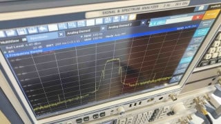
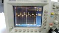
I am trying to get a project working where I am supplying data from an (Altera) FPGA's GPIO pins to a different reader device. I thought I could connect the 3.3v pins from the FPGA directly to the other system and be okay. At 5.8 MHz, where I need to be, there is a lot of ringing in my square waves. I am looking for a chip or configuration that will either condition the existing FPGA signal or more preferably a push-pull type line driver that will condition the signal from the FPGA, read it properly and output a clean square wave at 5.5-6 MHz. Attached is an image of the signal at the FPGA where the GPIO pin is only connected to my o-scope.
 

Attachments

digsys

Joined Jun 27, 2018
27
You probably do not have your scope probe connected properly and what you are seeing on the scope is an artifact.
...oooorrrr the probe hasn't been "tuned". Usually, there is a trimpot which you adjust against the ref square wave found on the scope ... or both
 

MrChips

Joined Oct 2, 2009
34,807
...oooorrrr the probe hasn't been "tuned". Usually, there is a trimpot which you adjust against the ref square wave found on the scope ... or both
No. It's a lot more than that but we're not going to tell you until you tell us more of what you have done to the scope and scope probe to get such an awful picture on the screen.

Edit: oops... sorry, I thought that you were the TS.
 

OBW0549

Joined Mar 2, 2015
3,566
The ringing you're seeing on that waveform is almost certainly caused by improper scope probe grounding.

Refer to Fig. 1.9 on p. 10 of the document @danadak linked to for an explanation of why this occurs and why using a probe ground lead as short as possible is needed to avoid what you are seeing.
Ringing.png
 

MrChips

Joined Oct 2, 2009
34,807
Ok, the cat has been let out of the bag.
Here is your problem.

1) Are you using a x10 probe set to the x10 option?

2) Is the probe ground clip properly connected to the proper ground point in your circuit?
 

danadak

Joined Mar 10, 2018
4,057
Are GPIO by chance driving power MOSFET gates, or other high
C loads ? Or just standard inputs to other CMOS devices ?

Regards, Dana.
 

Thread Starter

fmrPIC

Joined Nov 11, 2016
22
Thank you bunches. Here is what I did. Instead of waiting for responses, I redesigned my PCB and added several sn74l... push pull buffers last night. I now have the finished board on hold and I will wait until I see another mistake before getting it fabricated. I also mimicked the signal on TINA feeding the sn74l... and worked well.
Today, I looked at the forum and remembered that I have not tuned the o-scope probes recently. I made some adjustments and the square waves are much cleaner. The square waves are better now and it will save me 10 days of getting the board made and populated.
Because the signal is bouncing at both voltages, is that why people are screaming that I may not be looking at the signal?
 

danadak

Joined Mar 10, 2018
4,057
The ringing may or may not be symmetrical on a signal depending on current path
attributes the current is sourcer/sunk from. In this case looks symmetrical so source/
sink paths ~ equivalent.

Regards, Dana.
 
Top