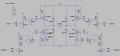
Big thanks to sghitoto for the circuit and everyone else for the information. According to a simulation:
M1 12-0V: ~3us
M1 0-12: ~85us
M3 0-12V: ~22us
M3 12-0V: ~135us
The worst case is about 10% of the 1ms switching period so I'm happy with this circuit for now. However, I want to confirm the switching times according to the FET datasheets. Can someone help with the algebra? The calculations I've found are overly complicated for my interests. I'm looking for the lightweight turn-on / turn-off formula.
As for controlling 4 lines instead of 2, I've been studying this chart from TI. I'm not sure which switching order will be best so I decided to keep 4 control lines. It makes the most sense to simply write ENABLEA or ENABLEB HIGH to provide a ground path then PWM the P channel FETs.
Uh oh, I think I replied to your question as if you were the thread starter.
I'll have to be more careful in the future, and thanks for telling me about this.
Big thanks to sghitoto for the circuit and everyone else for the information. According to a simulation:
M1 12-0V: ~3us
M1 0-12: ~85us
M3 0-12V: ~22us
M3 12-0V: ~135us
The worst case is about 10% of the 1ms switching period so I'm happy with this circuit for now. However, I want to confirm the switching times according to the FET datasheets. Can someone help with the algebra? The calculations I've found are overly complicated for my interests. I'm looking for the lightweight turn-on / turn-off formula.
As for controlling 4 lines instead of 2, I've been studying this chart from TI. I'm not sure which switching order will be best so I decided to keep 4 control lines. It makes the most sense to simply write ENABLEA or ENABLEB HIGH to provide a ground path then PWM the P channel FETs.
You might want to think about this a little more.
The 10k pullups are going to mean the gate can not charge or discharge very fast, meaning the switch times will be much longer than they could be. This is why dedicated mosfet driver chips are used. You get fast turn on and fast turn off, if that's what you really want of course.
You might want to think about a typical fast bridge circuit too. With mosfets you can do 100kHz which means each cycle is 10us long, and each half cycle is just 5us long, and yet the rise and fall times are still not too excessive.
What is it that you are trying to calculate, is it the predicted rise and fall times?
These switching times are usually simplified based on what they refer to as the 'gate charge'.
The calculations are not that complicated if you want to go through one or two examples.
NOTES:
The required switch time 't' and the total gate charge 'Qg' are related to the drive current 'ig':
t=Qg/ig
This implies a linear relationship although it is more exponential involving the gate voltage and the total drive resistance:
ig=(Vg/Rg)e^(-t/(RC))
and then you have to sum over time, but if you make sure the current is Vg/Rg you can get some reasonable results. This would mean:
t=Qg/(Vg/Rg)
where Vg is the gate voltage and Rg the drive resistance.
So the idea is to set the drive current as the required peak current.
You can get Qg from the data sheet normally but if not you can measure it.
Dedicated gate drive chips can help a lot here because they can supply a large current like 1 or 2 amps, and that will be good enough for applications that do not have to reach the maximum switching speed, while still obtaining a relatively fast switch time.
A quick calculation...
For gate charge Qg=200nC and Vg=5v and Rg=1000 Ohms we would do:
t=200e-9/(5/1000)=40us
With Rg=100 Ohms however we get:
t=4us
and with Rg=10 Ohms we get:
t=400ns
so you can see the difference Rg makes.
Note that Rg includes any internal gate resistance as well as the external gate resistor value.

 Facebook
 Google
 GitHub
 Linkedin