
So I'm running an ultra-low power design and a 0-10V dimming circuit is a part of it. All of the dimming circuits I've done using op-amps have all previously been sourcing current; however this time I'm trying to sink current (at a minimum of 58mA).
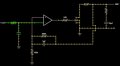
I'm currently using a simple op-amp circuit (TLV9XXXX Series) that runs rail to rail from 0-3.3V. As of right now, the circuit is taking a PWM signal straight from the micro. It passes through a high impedance path before it hits the inverting input. The output runs through just 270ohm resistor which passes to the gate of an NDS331 N-ch FET. The source of the FET is grounded and the Drain has a very low resistance pull-up; which branches to the feedback I have set up going back to the non-inverting input (just a parallel RC loop) with a mild pull down to ground (As shown in the photo I've attached).
I'm well aware that how much this 0-10V circuit can sink is up to the MOSFET; though I'm attempting to get the most linear relationship between the PWM input voltage (0-3.3V) and the output voltage (0-10V with min-dim at around 500-700mV) that I can while also also being able to sink a decent amount of current (in relation the rest of the project).
Right now, the value of the resistor at the drain of the MOSFET is 2.2ohms, along with the cross-line resistor that's in series with 10uF ceramic.
I know there are much easier ways to dim; I have another dimming circuit that runs off of an isolated low voltage transformer with a current mirror feeding an output FET but I'm trying to conserve energy on this one as well as run it from only one micro output (I'm running low).
Ultimately, I'm wondering if there is a better way to configure this set up (PS Sorry for the bad photo but LTSpice is no better lol).
Thanks")
I'm currently using a simple op-amp circuit (TLV9XXXX Series) that runs rail to rail from 0-3.3V. As of right now, the circuit is taking a PWM signal straight from the micro. It passes through a high impedance path before it hits the inverting input. The output runs through just 270ohm resistor which passes to the gate of an NDS331 N-ch FET. The source of the FET is grounded and the Drain has a very low resistance pull-up; which branches to the feedback I have set up going back to the non-inverting input (just a parallel RC loop) with a mild pull down to ground (As shown in the photo I've attached).
I'm well aware that how much this 0-10V circuit can sink is up to the MOSFET; though I'm attempting to get the most linear relationship between the PWM input voltage (0-3.3V) and the output voltage (0-10V with min-dim at around 500-700mV) that I can while also also being able to sink a decent amount of current (in relation the rest of the project).
Right now, the value of the resistor at the drain of the MOSFET is 2.2ohms, along with the cross-line resistor that's in series with 10uF ceramic.
I know there are much easier ways to dim; I have another dimming circuit that runs off of an isolated low voltage transformer with a current mirror feeding an output FET but I'm trying to conserve energy on this one as well as run it from only one micro output (I'm running low).
Ultimately, I'm wondering if there is a better way to configure this set up (PS Sorry for the bad photo but LTSpice is no better lol).
Thanks
Attachments
-
 57.5 KB Views: 40


