Facebook
 Google
 GitHub
 Linkedin
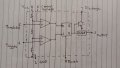
The Voltages for the two comparators inside the 555 are developed across a voltage divider consisting of three equal resistors R of 5K ohms each. The threshold comparator is referenced at 2/3 Vcc and the trigger comparator is referenced at 1/3 Vcc. The two comparators control the flip-flop, which, in turn controls the state of the output. When the timer is in the quiescent state, the internal transistor TI is conducting and represents a short circuit across timing capacitor C. The level of the output terminal is low. In most practical circuits, the-voltage on pin. 2 is held above the trigger point by a resistor connected to Vcc.
When the triggered input is in quiescent state, the corresponding comparator is at 0 state and thus the flip-flops remains in its initial 0 state. But when the triggered input changes to 1 state, the flip-flop outputs to 1. The Base of transistor is connected to Q output of flip-flop. When it changes to 1, it allow the capacitor to discharge.