Wien oscillator -- BIG problem

Thread Starter

hash

Joined Apr 27, 2007
15
Hello, I was wondering if you could help me with a project I have for school. I'm supposed to design a wien bridge oscillator but I'm not allowed to use an opamp, everything must be done using transistors.
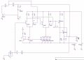
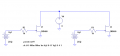
I took the differential amplifier schematic from another electronics class and tested it with pspice to see if it works, and it does what it's supposed to in a simple configuration (it outputs the signal correctly and with the correct gain).
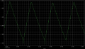
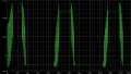
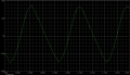
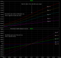
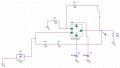
So far so good, but if I put it in a wien bridge configuration, no matter what values the RC network have, it oscillates around 1MHz with some distortion. I've tried a lot of things, including fiddling with the orcad simulator but to no avail. With the same settings (simulator and wien network) a database opamp (uA741) oscillates just fine, at the frequency set on the wien bridge. Therefore I'm guessing there's something wrong with the amplifier, but what?

I'm attaching the schematics and output/fft, maybe you can help...
 

Attachments

Thread Starter

hash

Joined Apr 27, 2007
15
Wow, that looks... uncomplicated :) thanks for the quick reply.
The frequency is variable between 3KHz-18KHz, and the automatic gain control has to be made using a jfet. These were supposed to be simple things to do after I would get the oscillator to behave.
One more thing, the load has to be 600 ohms, I see the circuit is made for loads greater than 3K.
 

Thread Starter

hash

Joined Apr 27, 2007
15
Well... I've read the fine print on the project details and it says that the total gain at the amplifier stage of the circuit must be over 10.000, that rules out the simple design you've shown me earlier :(
Still, I would like to know if you see something wrong with the amplifier. Or are the problems coming from orcad's pspice?
 

SgtWookie

Joined Jul 17, 2007
22,230
In Clipboard02.jpg, there is no current limiting resistor on the collector of Q9. If it happens to be conducting when Q5 through Q8 are also conducting, you will place a dead short across the rails.

I don't see why you need FOUR transistors in parallel (Q5-Q8), I would think that one should be sufficient - but I haven't modeled the circuit, either.

I don't quite get what you're doing with Q3 and Q4, either, but I haven't spent much time on it. Offhand, it doesn't make sense to have the ground above the collector of Q3, and then you have it's collector tied to the base.

In Clipboard03.jpg - is that simply a theoretically ideal operational amplifier model? Or is there a real-world op amp that it's supposed to represent?
 

studiot

Joined Nov 9, 2007
4,998
10.000 is the open loop gain of the amplifier. Not that difficult to achieve if you use darlingtons and a high impedance load.

For the Wein bridge to operate the closed loop gain must be exactly 3. Any less and there will be not oscillation, any more and there will be distortion or worse. This is set by your R1 and R2 in clipboard3.

For this reason either R1 or R2 must be made output dependant (eg your FET) You could make the other adjustable to just get the oscillator working correctly. Clipboard3 is in the correct configuration.
 

Thread Starter

hash

Joined Apr 27, 2007
15
well... Q3 - Q8 are tied up in a current mirror, Q3 sets the current to about 0.5mA (15V-0.6V/23.6k). So the current trough the first dif. amplifier stage is 2x0.25mA and trough the second amplifier stage is 2x1mA
I've played around with a some values but the oscillation frequency stays the same, at about 1MHz.
The opamp in clipboard3 is the one in clipboard2, with all the ports set (names on the red arrows).
 

Audioguru

Joined Dec 20, 2007
11,248
Opamps use a "frequency compensation" capacitor to prevent oscillation when negative feedback is applied. Most opamps have a frequency response that is flat from DC to only about 10Hz. Then the frequency compensation capacitor rolls-off the gain so it is less than 1 at a high frequency where the phase shift would cause oscillation.
 

Thread Starter

hash

Joined Apr 27, 2007
15
OK, DONE! :)
I've put a small capacitor (10nF) between the output and the final stage of the amplifier and it worked wonders, filtered all the very high frequency stuff.
Thanks guys !
 

hgmjr

Joined Jan 28, 2005
9,027
OK, DONE! :)
I've put a small capacitor (10nF) between the output and the final stage of the amplifier and it worked wonders, filtered all the very high frequency stuff.
Thanks guys !
So can you go ahead and post the final schematic of the working unit so that we can all see it?

hgmjr
 

Thread Starter

hash

Joined Apr 27, 2007
15
I've attached the schematic, it isn't pretty but it works at the desired frequency.
The problem now is the output signal wich looks more like a sawtooth than a sine wave...
 

Attachments

Thread Starter

hash

Joined Apr 27, 2007
15
The circuit exists only in orcad, if you are referring to a simulation with a 'standard' opamp, yes, it does more or less look like a sine wave, not a sawtooth wave (with uA741).
 

Audioguru

Joined Dec 20, 2007
11,248
The 22nF capacitor is 1000 times too big . It is cutting all the frequencies instead of just the very high frequencies.
Try 22pF across R3 instead.
 

Thread Starter

hash

Joined Apr 27, 2007
15
Here's what happens when I exchange the 22n with the 22p (and for that matter, any other value less than 10n)

LE: I've managed to strike a balance between the capacitor (10n) and the negative feedback network resistors. The output resembles a sine wave but the negative amplitude is less than the positive one. I suspect the cause being the diode which rectifies the negative part of the signal and takes 0.6V to work. -- s3.png shows the new output signal
 

Attachments

Ron H

Joined Apr 14, 2005
7,063
Your distortion is caused by slew rate limiting. R3 cannot supply enough current to your compensation cap to allow the output to slew as rapidly as it needs to.
I would try putting the compensation cap from base to collector of Q10.
Also, I think you need an N-channel JFET, or you need to reverse to polarity of D2. The resistance of the JFET needs to go up as the signal amplitude increases. You will also need a discharge path for C3. I think you'll discover that C3 needs to be much bigger if you want to use realizable values for the discharge resistor. For example, if you put 1Meg across your 1nF, the discharge time constant will only be 1ms.
I suspect you will run into other issues with the JFET, like harmonic distortion and amplitude stability, if you ever manage to get a semblance of a sine wave.:rolleyes:
 

Thread Starter

hash

Joined Apr 27, 2007
15
That capacitor between the base and collector of Q10 helped a little but I'm still getting heavy distortion if I drive the thing where I want to (I want it to output 3.3V, now at 1V it has low distortion).
The j-fet and diode network are ok, because it's p-type it needs negative voltage (rectified by the diode on the negative part of the signal) between gate and source to go into the linear region and change its resistance.
 

Ron H

Joined Apr 14, 2005
7,063
Negative gate-to-source voltage on a p-channel turns it on, not off. In fact, you are forward-biasing the gate junction. You need less gain as the amplitude increases. This means that the JFET resistance needs to increase.
Below is a sim of a representative PJFET. The part number is different, but the principle is the same.
 

Attachments

Top