Whats wrong with this circuit...?

Thread Starter

Himanshoo

Joined Apr 3, 2015
265
Hi guys...
I got some queries regarding this circuit..Lets go one by one....
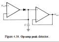
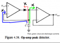
The text says..
"Input bias current causes a slow discharge (or charge, depending on the sign of the bias current) of the capacitor. This is sometimes called "droop," and it is best avoided by using op-amps with very low bias current "
As we know that the input bias currents are the residual currents which arises due to mismatch of internal fabricated transistors and are of the order of nanoamperes (100nA for LM324)..
My queries are...
1.In comparison of the signal voltage with input bias current ,the signal voltage have much larger magnitude..in order of volts ..hence it could easily overcome the effect of the input bias currents...and the effect of input bias currents could easily be neglected...Then why the author didn't neglect these?

2.Also to contradict the harms of input bias current there is a provision of providing the dc return resistor to ground....but in this figure it is absent...else the author tells to use opamp with very low bias currents as a remedy....can't we use DC return resistor ..??

Please help...
 

Attachments

MikeML

Joined Oct 2, 2009
5,444
The whole point of a peak detector is to hold the peak voltage forever (or at least until the next peak comes along...). Anything you do to cause the charge placed on the capacitor to leak away degrades the operation of the peak detector and compromises its ability to faithfully report what was the peak voltage that occurred x sec ago...

Leakage paths from the capacitor include its own internal leakage, the input bias current, and any shunting resistors you might put there in a misguided attempt to cancel the input bias current...
 

blocco a spirale

Joined Jun 18, 2008
1,546
This circuit just holds the peak input voltage at its output. That voltage is stored on C so you don't want C discharging into the inputs of the op-amps.

I don't know what you mean by a DC return resistor.
 
Last edited:

Jony130

Joined Feb 17, 2009
5,487
As we know that the input bias currents are the residual currents which arises due to mismatch of internal fabricated transistors and are of the order of nanoamperes (100nA for LM324)..
No wrong. Input bias current has nothing to do with input transistor mismatch.
As you should know every op amp has a differential amplifier at his input. And every transistor need a "base current" to work.
And this input bias currents is nothing more than input transistor base current (or reverse leakage current in FET's). And Input Offset Current is due to mismatch of a input transistors beta.
0.9.PNG
Also notice that if Ri = 100KΩ and Ib = 100nA and the op amp voltage gain is 10V we have a DC-offset at the output.
Vout_off = 100k*100nA * 10 = 10mV * 10V = 0.1V. And in some applications such a big offset is unacceptable.
 
Last edited:

crutschow

Joined Mar 14, 2008
34,283
If you use an op amp with very low input bias current, such as those with CMOS input transistors, than you will have low droop on the hold capacitor with time.
The capacitor droop in volts is [Vdroop = (Ibias * t) / C] where t is time and C is the capacitor value.
 

Thread Starter

Himanshoo

Joined Apr 3, 2015
265
Leakage paths from the capacitor include its own internal leakage, the input bias current, and any shunting resistors you might put there in a misguided attempt to cancel the input bias current...
Until and unless we are not providing any kind of shunting resistor to ground in order to cancel the input bias current...how can the input bias current paths could be responsible for the discharge of the capacitor...
I agree to you that the input bias current may charge the capacitor in long run of time..but how can discharging through it could be possible..as we know that the terminal of opamps are regarded as the input bias current paths and also..we know that no current flows through them..so then where would the discharge current go then.....?
// ignoring internal capacitor leakage for a moment
 

Attachments

Thread Starter

Himanshoo

Joined Apr 3, 2015
265
If you use an op amp with very low input bias current, such as those with CMOS input transistors, than you will have low droop on the hold capacitor with time.
The capacitor droop in volts is [Vdroop = (Ibias * t) / C] where t is time and C is the capacitor value.
Please clarify what is droop...
Is it the phenomenon of causing the capacitor to charge up by the input bias currents
or
It is the voltage by which capacitor gets charged due to the input bias currents ?
 

Thread Starter

Himanshoo

Joined Apr 3, 2015
265
No wrong. Input bias current has nothing to do with input transistor mismatch.
Hi Jony...
If input bias current has nothing to do with the transistor mismatch..the whats the need to cancel them ...
please refer to the following url...
https://e2e.ti.com/blogs_/archives/...cancelation-resistors-do-you-really-need-them

or if they are talking about cancellation of the input offset voltage then ...why they have named it "Input bias current cancellation resistors"
 

Jony130

Joined Feb 17, 2009
5,487
Hi Jony...
If input bias current has nothing to do with the transistor mismatch..the whats the need to cancel them ...
please refer to the following url...
https://e2e.ti.com/blogs_/archives/...cancelation-resistors-do-you-really-need-them
or if they are talking about cancellation of the input offset voltage then ...why they have named it "Input bias current cancellation resistors"
Yes, they are talking about cancellation of the input offset voltage caused by input bias current .
And here you have example
Case 1 - R3 was not chosen properly and this will cause a large DC-offset.

20.png

Case 2 - R3 = R1||R2 no DC-offset at the output.
21.png

As for peak detector you are right, we need some kind of reset circuit.
 

Attachments

Last edited:

crutschow

Joined Mar 14, 2008
34,283
Please clarify what is droop...
Is it the phenomenon of causing the capacitor to charge up by the input bias currents
or
It is the voltage by which capacitor gets charged due to the input bias currents ?
Yes to both.
Droop is the change in capacitor voltage (either up or down depending upon the direction of the bias current) caused by the op amp bias current during the hold period, since this current has to be provided from the charge on the capacitor.

You seem be confusing bias current with bias offset current (the difference between the bias current of the two inputs).
The latter is caused by transistor mismatch and cannot be readily compensated.
But the bias current (not including the offset) can be compensated in a voltage amp configuration by making the external impedance of both op amp inputs the same.

Note that the bias current causing the capacitor droop cannot be readily compensated, which is why you need a low bias current op amp.

This is completely separate from input offset voltage which causes its own additional error and also cannot be readily compensated unless a pot is added to provide an adjustable cancelling offset.
 

Thread Starter

Himanshoo

Joined Apr 3, 2015
265
You seem be confusing bias current with bias offset current (the difference between the bias current of the two inputs).
Yes i got it...thanks
actually the cancellation is meant to be of the input offset voltage ...and the input bias offset current are the current which cause the input offset voltage to develop across the input resistors....

lots of inputs:)
 

crutschow

Joined Mar 14, 2008
34,283
Yes i got it...thanks
actually the cancellation is meant to be of the input offset voltage ...and the input bias offset current are the current which cause the input offset voltage to develop across the input resistors....
You still seem to be confusing two different things.
Yes, the input bias current can cause an offset voltage at the output but that's independent and separate from the input offset voltage, which adds it's own offset at the output.
You can see each is specified separately in an op amp's data sheet.
 

Thread Starter

Himanshoo

Joined Apr 3, 2015
265
And this will charge or discharge the capacitor.
opamp peak detector.png
What i am not getting is that..as opamp is fundamentally a voltage device and due to its very high input impedance no current actually flows through its input terminals.... so as in the figure the discharge current can't go in any of the directions shown by the arrows ..and since there is no shunting resistor ...then where actually the discharge current will manifest itself...?
 

Jony130

Joined Feb 17, 2009
5,487
You simply need some kind of discharge "switch" or resistor because op amp bias current is very low so you will have to wait very long time before capacitor is discharge.
 

crutschow

Joined Mar 14, 2008
34,283
View attachment 92543
What i am not getting is that..as opamp is fundamentally a voltage device and due to its very high input impedance no current actually flows through its input terminals.... so as in the figure the discharge current can't go in any of the directions shown by the arrows ..and since there is no shunting resistor ...then where actually the discharge current will manifest itself...?
Not true.
The input impedance is indeed high, but the bias current is an actual current that flows in/out of the input terminals (rather like a high impedance current source).
What do think it is if not a real current?
 
Last edited:

Veracohr

Joined Jan 3, 2011
772
opamp is fundamentally a voltage device and due to its very high input impedance no current actually flows through its input terminals
But a little current DOES flow into the input terminals: the bias current that is being discussed. That's what causes the voltage droop/slow discharge of the capacitor.
 
Top