What's wrong with this boost converter?

Thread Starter

k1ng 1337

Joined Sep 11, 2020
960
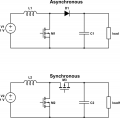
Hi in the attached image M3 is connected so that it is conducting in both ON and OFF states, what can be said about the MOSFET in these states and it's corresponding algebra?

Is it reasonable to say that while M3 is OFF it can modeled as a diode and when ON a resistor? I tested both p and N channel and observed a .5v drop while each MOSFET was off when reverse biased.

Thanks :)
 

Attachments

Last edited:

Thread Starter

k1ng 1337

Joined Sep 11, 2020
960
Hi I've built both boost converters in the attached image. The asynchronous was a success, 85%+ efficiency. To drive the MOSFET I used a BJT totem poll push pull, however when I replaced the diode with the complementary p channel MOSFET, the circuit output less power and got hot both at high and low duty cycle.. what's the problem? I suspect M3's gate is not being driven correctly.

Vin 5v
D1 2n5819
M 1,2 irf540
M3 irf9540
C 1,2 1uF
L 1,2 250uH (4x 1/4W 1mH in parallel)
Load - DC motor

MOSFETs are driven by BJT NPN and PNP totem poll push pull, I tested the circuit prior and it behaves as expected.

Thanks :)
 

Attachments

Veracohr

Joined Jan 3, 2011
772
If both FETs are on at the same time, the low side one will sink current both from the input and the output capacitor. Check the gate drive signals.
 

Tonyr1084

Joined Sep 24, 2015
7,899
It could be the time it takes for one FET to turn off before the other turns on. Thus, two may be on ever so briefly but still draw a lot of current. Remember, FETs (MOSFETs) have a capacitance built into their gates. If you don't pull them down to ground fast enough it is still on during the time it takes for the gate to be pulled fully to ground (or V+, depending on the FET).
 

AnalogKid

Joined Aug 1, 2013
11,038
What other information do you need?
To paraphrase Rear Admiral Joshua Painter, an engineer don't tak a dump, son, without a schematic.


This is a help forum. You are here because there is something about your design or build that you think you know, but you don't. Since you already have built the circuit, I assume you have a complete schematic. Without one ...

He who loves practice without theory is like the sailor who boards ship without a rudder and compass and never knows where he may cast.
- Leonardo DaVinci

ak
 

neonstrobe

Joined May 15, 2009
190
Yes, timing. The PMOS needs to turn on fractionally after the NMOS is turned off, and off fractionally before the NMOS is turned on i.e. non-overlapping drive signals.
 

Thread Starter

k1ng 1337

Joined Sep 11, 2020
960
It could be the time it takes for one FET to turn off before the other turns on. Thus, two may be on ever so briefly but still draw a lot of current. Remember, FETs (MOSFETs) have a capacitance built into their gates. If you don't pull them down to ground fast enough it is still on during the time it takes for the gate to be pulled fully to ground (or V+, depending on the FET).
To paraphrase Rear Admiral Joshua Painter, an engineer don't tak a dump, son, without a schematic.


This is a help forum. You are here because there is something about your design or build that you think you know, but you don't. Since you already have built the circuit, I assume you have a complete schematic. Without one ...

He who loves practice without theory is like the sailor who boards ship without a rudder and compass and never knows where he may cast.
- Leonardo DaVinci

ak
You remind me of a teacher who wouldn't answer a question unless it was asked with perfect syntax and would belittle the student for his choice of words rather than simply share his knowledge. I would prefer you don't post in my threads if you can't give insight without the ego, I'm asking about a MOSFET in a simplified schematic not da Vinci...

Yes, timing. The PMOS needs to turn on fractionally after the NMOS is turned off, and off fractionally before the NMOS is turned on i.e. non-overlapping drive signals.
How would I go about controlling this? I analyzed the datasheets and the P channel is generally slower, what parameters in the datasheet govern these times?

Perhaps I should give each MOSFET its own gate driver? I assumed using a single push pull would force the FETs to synchronize at the sake of additional turn on / off times of the BJTs
 

Tonyr1084

Joined Sep 24, 2015
7,899
You remind me of a teacher who wouldn't answer a question unless it was asked with perfect syntax and would belittle the student for his choice of words rather than simply share his knowledge. I would prefer you don't post in my threads if you can't give insight without the ego, I'm asking about a MOSFET in a simplified schematic not da Vinci...
If this is directed at me - my apology. I didn't realize I was speaking (or being taken) in that tone. I will refrain from any further comment.
 

Thread Starter

k1ng 1337

Joined Sep 11, 2020
960
If this is directed at me - my apology. I didn't realize I was speaking (or being taken) in that tone. I will refrain from any further comment.
I was referring to analogkid, so far everyone on this site has been great.. I don't expect the answer just insight and I would rather have 10 opinions of what is going on that I can investigate myself over a specific answer that demands significant trial and error
 

Veracohr

Joined Jan 3, 2011
772
You remind me of a teacher who wouldn't answer a question unless it was asked with perfect syntax and would belittle the student for his choice of words rather than simply share his knowledge. I would prefer you don't post in my threads if you can't give insight without the ego, I'm asking about a MOSFET in a simplified schematic not da Vinci...
It’s unfortunately common on this forum.


How would I go about controlling this? I analyzed the datasheets and the P channel is generally slower, what parameters in the datasheet govern these times?

Perhaps I should give each MOSFET its own gate driver? I assumed using a single push pull would force the FETs to synchronize at the sake of additional turn on / off times of the BJTs
Integrated dc-dc converters have the circuitry to minimize this. I’d recommend finding a synchronous controller IC instead of trying to build one from scratch.
 

Thread Starter

k1ng 1337

Joined Sep 11, 2020
960
It’s unfortunately common on this forum.


Integrated dc-dc converters have the circuitry to minimize this. I’d recommend finding a synchronous controller IC instead of trying to build one from scratch.
At this point in my learning I think I'm better off utilizing the diode configuration and mastering that before trying to synchronize switches, half the fun is building it from scratch and seeing it come to life.. I do have a knack for trying to reinvent the wheel
 

AnalogKid

Joined Aug 1, 2013
11,038
Well, so much for humor.
You remind me of a teacher who wouldn't answer a question unless it was asked with perfect syntax and would belittle the student for his choice of words rather than simply share his knowledge.
If you re-read this thread, you will see that that is not what is going on here. Also, you can see in my body of work that I regularly comment on other posters, especially senior ones, for being prissy about style over content. And about 555's, but that's another topic. My issue with your question is that it is missing important content.

Nothing is more critical to an answer than the *quality* of the question. This is an electrical engineering question-and-answer forum, and you have a question about how a circuit is performing. Why is it so difficult to grasp the necessity, if not just usefulness, of a complete schematic? Your schematic has the answer to your question.

ak
 

neonstrobe

Joined May 15, 2009
190
There are two ways I have done this without IC's. One circuit I call a "multimultivibrator" is based on a conventional multivibrator but has two additional transistors switched by two additional capacitors from the original ones, but with slightly lower timing resistors. These turn off just before the main multivibrator changes state, giving a dead interval which can be adjusted by changing the secondary timing resistors. Another uses a single oscillator, diode and resistor fed delay stages (normal RC delay but with diode so that the "off" time is quick, only the "on" is slow) followed by a Schmitt trigger to give a clean pulse, one of these delay-trigger circuits on each side of the oscillator output so that the net two anti-phase signals have the dead zone.
The first circuit works OK but the second idea, a bit more complicated, gives better timing control.
The delay time you need is determined from the MOS switching times, which depends on the impedance you feed the gate with unless it is very low and you can provide a high gate current pulse (but we're only talking a few tens to hundred mA). The very fast switching times possible then may be impacted by wiring connections etc, so good efficiency needs careful wiring.
 

Thread Starter

k1ng 1337

Joined Sep 11, 2020
960
There are two ways I have done this without IC's. One circuit I call a "multimultivibrator" is based on a conventional multivibrator but has two additional transistors switched by two additional capacitors from the original ones, but with slightly lower timing resistors. These turn off just before the main multivibrator changes state, giving a dead interval which can be adjusted by changing the secondary timing resistors. Another uses a single oscillator, diode and resistor fed delay stages (normal RC delay but with diode so that the "off" time is quick, only the "on" is slow) followed by a Schmitt trigger to give a clean pulse, one of these delay-trigger circuits on each side of the oscillator output so that the net two anti-phase signals have the dead zone.
The first circuit works OK but the second idea, a bit more complicated, gives better timing control.
The delay time you need is determined from the MOS switching times, which depends on the impedance you feed the gate with unless it is very low and you can provide a high gate current pulse (but we're only talking a few tens to hundred mA). The very fast switching times possible then may be impacted by wiring connections etc, so good efficiency needs careful wiring.
Let's say I have two MOSFETs identical in every way, could I control the turn on and off time with the proper combination of pull up and pull down resistors giving them each unique timing because if I were to short the gates would they not turn on at the exact same time ideally speaking?
 

neonstrobe

Joined May 15, 2009
190
Not sure what you are asking here. If they have joined up gates they will turn on and off together - but we always include gate resistors to stop oscillations, in practice, though these need not be large. The problem is that during the switching they will both be on and in a push-pull converter or a converter with a synchronous rectifier, we need phased signals so that the overlap time is minimised. Getting the timing right is key to efficiency. Too long a delay could allow large inductive spikes to form; too slow and the efficiency goes to pot. IC controllers sometimes allow for the time delays to be adjusted for optimum performance.
 

jpanhalt

Joined Jan 18, 2008
11,087
Let's say I have two MOSFETs identical in every way, could I control the turn on and off time with the proper combination of pull up and pull down resistors giving them each unique timing because if I were to short the gates would they not turn on at the exact same time ideally speaking?
You can control the turn on time with resistors, but that is not a good way to do it, because the slower turned on mosfet will be in its linear conduction portion longer and create a lot more heat.

The way to prevent "shoot through" (i.e., both on at the same time) is to use appropriate drivers to turn each mosfet on or off quickly, but introduce a time delay between the signals. You can do that with discrete components, but it is far easier to use an MCU or purpose-designed chip.
 

Thread Starter

k1ng 1337

Joined Sep 11, 2020
960
You can control the turn on time with resistors, but that is not a good way to do it, because the slower turned on mosfet will be in its linear conduction portion longer and create a lot more heat.

The way to prevent "shoot through" (i.e., both on at the same time) is to use appropriate drivers to turn each mosfet on or off quickly, but introduce a time delay between the signals. You can do that with discrete components, but it is far easier to use an MCU or purpose-designed chip.
The simplest solution I've found is this RC network, I did some math and I could create an appropriate dead zone but I will need to invert one output therefore increasing the overall timing? Plus each out will drive a push pull network each.. what parameters govern all these times in the datasheet and how do I create the overall equation?

Parameters like Td(on), Td(off), rise and fall? The more logic and transistors I add seems to severally complicate the math
 

Attachments

Last edited:
Top