What's inside the Memory Chip in a DDR module?

Thread Starter

Electronic_Maniac

Joined Oct 26, 2017
253
Hi,

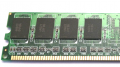
The following is a 1Gb DDR memory module. I would like to know how the bits are stored in the chips?
Like since it is a DRAM, where are the capacitors in the module?
And what are present in the chip? Are memory registers present in the chip?
Please explain.

Thanks.


upload_2018-1-9_11-59-27.png
 

Marley

Joined Apr 4, 2016
502
I can't see from the photo but look at the part number on each IC and Google that number. With any luck you will be able to find the chip's data sheet which will explain the organization of the memory cells on the chip. You may find that each IC stores 1G x 1 bit or possibly 512M x 1 bit. The array of ICs on the card makes up the stored byte.

This is dynamic RAM (DRAM) so each memory cell (each bit) will be a single MOSFET transistor. The state of each bit is stored as a charge on the insulated gate. This charge slowly leaks away so each bit has to be read and refreshed regularly.
 

dl324

Joined Mar 30, 2015
16,911
Have you tried Google?

All DRAM designs are going to be similar. A memory array arranged as a 2D matrix of transistors with logic to decode rows and columns, a sense amplifier to determine current state, and spare arrays that are fused in at test to replace defective portions.
 

AnalogKid

Joined Aug 1, 2013
11,037
In its most simple form, bits are stored as charge in a capacitor. If the charge is below a certain threshold value it is called a 0, and if the charge is above a threshold value it is called a 1. Like all capacitors, these are formed by two parallel plates. However, one of the plates is in fact the gate of a MOSFET. This saves space and energy. It is the output of the MOSFET that is tested to determine if the capacitor is holding a 0 or a 1.

It is difficult to describe just how small the capacitor and MOSFET are. There are billions of them in a space that is 1/4 the size of a postage stamp. There are no "memory registers" in the traditional sense because they take up too much room. A static ram bit cell takes 4 or 6 full sized transistors, while a dynamic ram bit cell takes only 1 transistor that definitely is not normal in its construction. There are input and output registers at the chip level to hold the data that is being read or written.

ak
 
Last edited:

Thread Starter

Electronic_Maniac

Joined Oct 26, 2017
253
I can't see from the photo but look at the part number on each IC and Google that number. With any luck you will be able to find the chip's data sheet which will explain the organization of the memory cells on the chip. You may find that each IC stores 1G x 1 bit or possibly 512M x 1 bit. The array of ICs on the card makes up the stored byte.

This is dynamic RAM (DRAM) so each memory cell (each bit) will be a single MOSFET transistor. The state of each bit is stored as a charge on the insulated gate. This charge slowly leaks away so each bit has to be read and refreshed regularly.
Sir, in your last para, you are saying that each bit is stored as a charge on the insulated gate.

Are you referring to a floating gate MOSFET or a capacitor connected to a MOSFET?
 

Thread Starter

Electronic_Maniac

Joined Oct 26, 2017
253
In its most dimple form, bits are stored as charge in a capacitor. If the charge is below a certain threshold value it is called a 0, and if the charge is above a threshold value it is called a 1. Like all capacitors, these are formed by two parallel plates. However, one of the plates is in fact the gate of a MOSFET. This saves space and energy. It is the output of the MOSFET that is tested to determine if the capacitor is holding a 0 or a 1.

It is difficult to describe just how small the capacitor and MOSFET are. There are billions of them in a space that is 1/4 the size of a postage stamp. There are no "memory registers" in the traditional sense because they take up too much room. A static ram bit cell takes 4 or 6 full sized transistors, while a dynamic ram bit cell takes only 1 transistor that definitely is not normal in its construction. There are input and output registers at the chip level to hold the data that is being read or written.

ak
Thanks sir. Now, I understand that the basic/fundamental unit inside a DRAM chip is a Capacitor and a switch (MOSFET),

and then comes the sense amplifier.

Am I right sir?
 

WBahn

Joined Mar 31, 2012
30,045
A MOSFET can be used as a capacitor. The source-drain regions are connected together and act as one terminal (with the channel being the plate) and the gate is the other plate. The thin oxide of the gate results in very high capacitance per unit area. Unfortunately, the capacitance is also quite nonlinear, but for memory that doesn't really matter.

DRAM chips have used a number of different topologies including vertical trench capacitors and I don't know if all of them can be described as FET capacitors. But that's largely beside the point -- however it is implemented, the idea is that you have a leaky capacitor on which a charge is stored. The sense amplifier (again, different approaches have been used over time) typically tries to weakly pull the capacitor to a mid level and detects whether the capacitor is charging or discharging in response. The capacitors are organized in an array allowing a given word to be selected.

Most DRAM modules have a fair amount of logic in them to handle refresh and burst modes of operation and there are registers associated with this logic, but these are not used for storage of the memory contents.
 

Thread Starter

Electronic_Maniac

Joined Oct 26, 2017
253
A MOSFET can be used as a capacitor. The source-drain regions are connected together and act as one terminal (with the channel being the plate) and the gate is the other plate. The thin oxide of the gate results in very high capacitance per unit area. Unfortunately, the capacitance is also quite nonlinear, but for memory that doesn't really matter.

DRAM chips have used a number of different topologies including vertical trench capacitors and I don't know if all of them can be described as FET capacitors. But that's largely beside the point -- however it is implemented, the idea is that you have a leaky capacitor on which a charge is stored. The sense amplifier (again, different approaches have been used over time) typically tries to weakly pull the capacitor to a mid level and detects whether the capacitor is charging or discharging in response. The capacitors are organized in an array allowing a given word to be selected.

Most DRAM modules have a fair amount of logic in them to handle refresh and burst modes of operation and there are registers associated with this logic, but these are not used for storage of the memory contents.
thank you sir
 
Top